I met with Bassam Hamaisi to ask him what is being done there at the university.

I met with Bassam Hamaisi to ask him what is being done there at the university.
Bassam, originally from Kfar Kana near Nazareth, currently lives in Tel Aviv. He acquired his academic education at Tel Aviv University in the field of electrical engineering. These days he is carrying out his doctoral thesis in the laboratory of Dr. Eran Sefer in the Faculty of Engineering at Tel Aviv University. His main interest is in the design of integrated circuits for work in the field of very high radio frequencies.
Bassam, so what are you doing there?
In our laboratory we develop integrated circuits for operating frequencies in the radio field, which are extremely high operating frequencies. These are millimeter and sub-millimeter wavelength waves, which are the shortest waves used in wireless communication today.
What is it actually about? Who uses it?
The goal is to transmit information wirelessly. Today, for example, in WiFi technology, the transmission rate is 2.4GHz. If you want to transfer a larger amount of information at a given time, for example send a movie at a rate of 5Gbyte per second, it is advisable to develop faster technologies. The problem is that the normal circuits and the components from which they are composed are not adapted to work at such high rates and will not be able to provide the required power.
There are quite a few interesting applications for the high-speed circuits we develop. For example, to quickly download movies or files from the Internet to mobile devices. Another example is in the field of imaging for security uses - to detect hidden weapons, or for medical applications such as cancer diagnosis. I will expand on the topic of imaging later.
So what is special about your approach to developing the circuits?
First, it is worth briefly mentioning what a transistor is. This electrical component is one of the important building blocks used, for example, to build a computer. The transistor is an electrical switch spring that has two states - it transmits or does not transmit an electric current. With the help of these components it is possible to implement all the logical functions ('and', 'or', etc.) that are required for the design of the computer's processor or memory units. The currently accepted technology for designing integrated circuits is called CMOS and is (usually) based on silicon transistors connected in a special way.
The currently common approach to developing electric circuits to work at high frequencies is the use of special and very fast transistors. These transistors are usually not made of silicon (but, for example, of GaAs), and they have a special structure and are quite expensive. Our goal is to use the popular CMOS technology to develop those circuits. The advantages of this approach are the cheaper price, the compatibility with the existing technology (therefore it is easier to integrate it in other circuits) and the fact that most factories are adapted to the production of circuits with this technology.
It must be remembered that one against one, the fast transistors will have better performance. Our goal is to find ways to get the best possible performance out of CMOS circuits for high frequency operation, so that we can compete cost-effectively with the expensive transistors.
Tell me what you're working on.
One of the projects I'm working on is high frequency imaging. A transmitter sends waves on a certain body and the reflected waves are collected by the receiver. Later, the information is processed into an image of the body on which the waves were sent (similar to imaging using acoustic waves or X-rays). Each pixel in our component is a transmitter-receiver that sends a wave that is partially absorbed and partially reflected from the scanned body. The intensity of the wave that returned to the receiver from a certain point indicates the (dielectric) properties of the material at that point. In this way it is possible to obtain a mapping of the properties of the material at any point. A future use of the technology is, for example, a non-invasive, safe (non-ionizing radiation) and fast diagnosis of skin cancer or tooth decay.
The advantage of using a high frequency wave is that the higher the frequency, the more the antennas inside the chip will be able to emit a smaller beam. This fact will allow us to use smaller pixels and get a higher resolution for the imaging device.
The challenge is to design the same transmitter-receiver pixel circuit in CMOS technology, which is not necessarily optimal for working at high frequencies, in an intelligent way so that the performance of the circuit will be good enough for commercial uses.

Tell me one of the tricks. how do you do it
I will give you an example: to transmit at a high frequency we need an electrical signal source that the signal it produces oscillates at the desired frequency. Suppose, for example, that we want to design a source at 300GHz. One possibility is to build a circuit with a fast and expensive transistor that can withstand these frequencies. A second option is to build a circuit using less good transistors, but to excite the circuit with slower oscillations, for example at 100GHz.
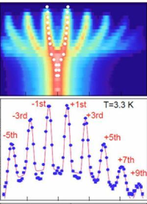
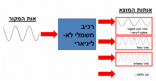
The secret is that these transistors have non-linear effects, that is, if I excite them with a signal of a certain frequency, their output signal changes at the original frequency but also at higher frequencies (see Figure 3). One of the higher frequencies that will arise is the 300GHz we are interested in. We need to make sure that the power of the high frequency oscillations that have arisen is strong enough for our applications. Therefore, the challenge is to build the circuit so that it results in optimal utilization of the secondary frequency in which we are interested. This way we can reproduce the performance of the expensive transistors.

What is the nature of the work? How did you achieve good performance?
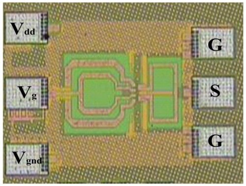
The first step is to take the designed circuit on paper and then test and improve it using simulation software. After you get good performance in the simulation, you switch to another software where you already design the integrated circuit on the computer, down to the smallest details including structure and materials (in layout parlance). After completing this step, the circuit is sent to production, and when it returns, it is characterized using the advanced test equipment we have in the laboratory to see if it does meet expectations.
One of the problems is that the existing models in the simulation software are not accurate enough to calculate the operation of the transistors at such high frequencies. For example, it happened to me that I sent a circuit that was designed to operate at a frequency of 240GHz, but when we received it it turned out that it produces oscillations at only 230GHz. At this stage, if necessary, some improvements can be made, that is, a new and more accurate circuit can be designed and manufactured.
At the end of the work process we get a circuit with better performance than the circuits of other research groups. So we publish the findings with an emphasis on the design form and advantages, and anyone interested can use our circuit for their work.
What's next?

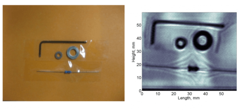
As I said, the long-term goal of the project is to build a transceiver for imaging purposes. In the meantime we managed to build the transmitter, and to test it we collaborated with another research group from Germany that built a receiver. Although their receiver is based on a different idea, the circuit is also produced in CMOS technology. We were able to show beautiful imaging results (see image 4). The next step in this project is to build a shelter with our technology.
————————————————————
I would be happy to meet and talk with any research student (maybe you?) who is willing to participate and tell me a little about what he is doing (and all for the price of a not too long conversation). You can contact me via Contact Us Form.
It's time to tell everyone what you're doing, maybe this time they'll understand too
The article was published on Oren Shaya's blog.to a constant extent"

6 תגובות
So you can make millions of such circuits, and make a health fund at home! The fact is that it's CMOS, so it's a beautiful, promising and cheap solution! Good luck, Bassam.
One more thing, to those who wrote the comments unrelated and out of place, please keep the discussion within the scope of science and not write nonsense!
And not Haifa University?
I'm sure the parents are disappointed.
Beautiful! The field of biosensors based on high frequency circuits attracts a lot of companies today,
The problem is the performance of these systems, I suppose that thanks to such studies it is possible to really improve the performance,
Best regards,
emir
Interesting research. From my knowledge in the field of circuits, the research on high-frequency circuits is a lively research in academia in the United States and attracts constant momentum and acceleration, good luck.
Interestingly, such chips have many applications in the field of imaging
It's a shame that more Arabs don't deal with science instead of crime and terrorism, there could have been real peace and prosperity.