Graphene - the most perfect atomic lattice of all

A thin layer of ordinary carbon, one atom thick, underlies this year's Nobel Prize in Physics. The two researchers Andre Geim and Konstantin Novoselov have shown that carbon with such a flat shape has unusual properties that originate from the amazing world of quantum physics.
Graphene is one form of carbon. As a material it is completely new - not only is it the thinnest, it is also the strongest. As an electrical conductor, its performance is similar to that of the metal copper. As a heat conductor it is superior to all other known materials. It is almost completely transparent, but at the same time it is so dense that even helium, the smallest gas atom, cannot pass through it.
As a result, the article about graphene, published in the prestigious journal Science in October 2004, caused a great stir throughout the world's scientific community. On the one hand, the unique properties of graphene allow scientists to examine the theoretical foundations of physics. On the other hand, a variety of possibilities for practical applications of the material are now emerging, including the preparation of new materials and the development of innovative electronic components. Carbon, the basis of all life forms on Earth, surprised us again.
Pencil, paper and glue
Nothing should have been easier than getting graphene, the wonder material derived from the ordinary graphite found in pencil tips. However, the most obvious and simple things are sometimes hidden from view.
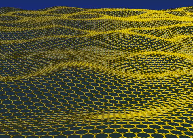
Graphene consists of carbon atoms connected together in a flat network pattern - similar to a honeycomb structure, but with a thickness of a single atom. In fact, one millimeter of graphite contains three million layers of graphene stacked one on top of the other. The layers are loosely connected and therefore can be easily separated and broken. Anyone who has ever tried writing with a pencil knows this experience, and it is possible that in this action, in fact, a single layer of atoms - graphene - remained on the paper.
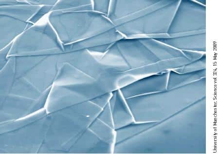
That's what happened when the two researchers used duct tape to remove thin layers from a larger block of graphite in a more methodical-scientific manner. At first they got flakes of material that contained many layers of graphene, but when they ran their paste-tear method ten or twenty times the flakes got thinner and thinner. The researchers' next step was to find the smallest segments of graphene among the thin layers of graphite and other forms of carbon. Here the second brilliant idea popped into their minds: in order to be able to see the findings of their painstaking work, the researchers from Manchester decided to anchor the resulting layers to a surface of zinc oxide - the usual material used in the semiconductor industry.
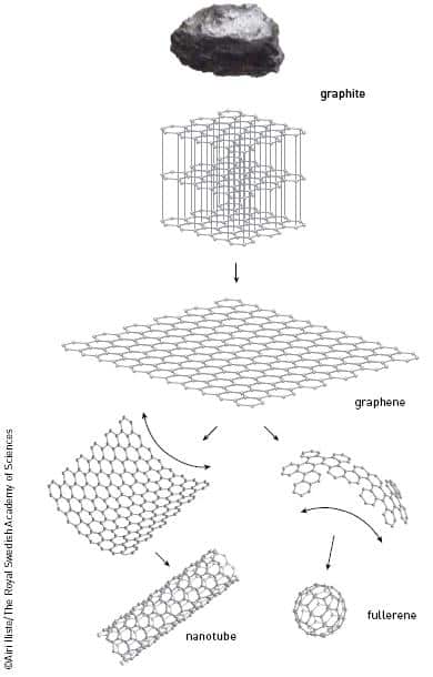
When the surface is placed under a normal microscope, a rainbow of colors can be seen, similar to the appearance obtained when oil is poured into water, and thus they were able to determine the number of graphene layers in the material. The thickness of the formic oxide surface, it turned out later, was critical to the discovery of graphene. Under the microscope, the clear structure of graphene has now been revealed - a true two-dimensional crystalline substance that exists at room temperature. Graphene is a perfectly ordered network of carbon atoms with only two dimensions, length and width. The basic unit of this pattern consists of six carbon atoms bonded together chemically. Graphene, like other known forms of carbon (fullerene and nanotubes) contains billions of carbon atoms bound together in a hexagonal pattern.
Awaiting discovery
It goes without saying that graphene has always existed; The limiting factor was the ability to distinguish it. Similarly, other natural forms of carbon appeared before scientists observed them clearly: first nanotubes and then hollow spheres of carbon - fullerenes (for which the Nobel Prize in Chemistry was awarded in 1996). The graphene, being trapped and hidden inside the graphite, was waiting to be discovered (photo 2). No one really believed this was possible.

Many scientists believed that it would be impossible to isolate such tiny substances: they would be crushed or destroyed at room temperature, or even simply disappear altogether. Despite these voices, a number of scientists continued to try, despite the fact that previous attempts to obtain pure graphene had failed. At this point in time it was possible to obtain layers with a thickness of less than a hundred atoms - indeed, some of them were so thin that they appeared transparent.
One of the ways to obtain graphene from graphite is to insert chemical substances between the layers of atoms in order to weaken the bond between them and the layers around them. Another method is to simply scratch and lightly peel off the layers of graphite. Also, they tried, and with success, to "burn" and evaporate out the tin from crystals of carbide tin. At high temperatures thin layers of carbon remain. Different methods of epitaxial growth, which are used to produce a variety of semiconductor materials, are the most promising methods of producing graphene for use in the electronics industry. Graphene surfaces with a width of 70 cm are the largest graphene materials created to date.
In a world of paradoxes
The researchers were only able to obtain microflakes of the new material. Despite their extremely small size, they could now begin to examine two of graphene's unique properties, both of which affect its electronic properties.

The first feature is the pure composition of graphene. The perfect arrangement originates from the strong bond between the carbon atoms. At the same time, the knots are flexible enough to allow stretching of the net up to 20% of its original size. The ordered lattice also allows electrons to move along it great distances without any interference (no electrical resistance). In normal conductors, electrons are often "bounced" from place to place and this form of transfer weakens the performance of the material as a conductor.
Another unique property of graphene lies in the fact that the electrons in it behave like light particles, massless photons, which move in a vacuum at a speed of 300 million meters per second. Quite similarly, electrons moving inside the graphene behave as if they have no mass and move forward at a constant speed of a million meters per second. These features promote the possibility of examining certain phenomena more easily on a smaller scale, that is, without the need for a complex particle accelerator.
Graphene also allows scientists to examine some of the more surprising quantum phenomena that have until now only been discussed in theoretical terms. One of these phenomena is a form of Klein tunneling formulated by the Swedish physicist Oscar Klein in 1929. The result of tunneling in quantum physics describes how particles are sometimes able to pass through barriers that normally would not succeed. The bigger the barrier, the less chance quantum particles will pass through. However, this rule does not apply to the electrons moving inside graphene - under certain circumstances they move forward as if the barrier did not exist at all.
dream worlds
The possible practical applications for graphene have received much attention. Until now, most of them exist only in our vision, but many of them are already being tested, even by the two Nobel laureates themselves.
Graphene's conductivity is responsible for much interest in this material. The scientists predict that graphene-based transistors will be significantly faster than those currently produced by Zoran. In order for computer chips to become faster and more energy efficient, they must become smaller. The idea of using a mold already reaches its size limits, when the material stops functioning as required. The threshold limit for graphene is even lower, so graphene-based components can be stacked on a chip more densely and efficiently.
The scientists reached one milestone a few years ago when a key component, the graphene transistor, was developed that is as fast as its silicon-based counterpart. It is possible that we are now on the verge of further miniaturization of the electronic components that will lead to increased efficiency in the computers of the future. Today, graphene computers are little more than a pipe dream, although transparent, paper-thin, foldable computer displays are already being developed for electronics in the near future.
In the meantime we can only speculate what some of those applications will be, more or less practical, all of which will require further research.
Since graphene is practically transparent (up to almost 98%) and is also able to conduct electricity, it should be suitable for the production of transparent touch screens, lighting panels and possibly even solar cells. Also, it will be possible to use plastic as electronic components if we add only one percent of graphene to them. Similarly, adding a small proportion of graphene to plastic increases its resistance to heat by about 30 degrees Celsius while also making it harder. This feature could be used for the development of innovative materials that are extremely strong, which will also be thin, flexible and light-weight. In the future, it will be possible to make satellites, airplanes and cars from these innovative materials.
The perfect structure of graphene also makes it suitable for the production of extremely sensitive sensors that can detect the lowest levels of pollutants. It will be possible to measure the adsorption of even a single particle.
Serious game
The list of possible applications of graphene is long. The feverish activity that began following the discovery of the substance graphene will eventually yield results. No one can predict what the future will bring, not even this year's laureates. They allowed themselves to walk one by one in a maze of possibilities and they had the luck and the knowledge to grasp the opportunities that appeared before them - as we know opportunities appear only to those who are ready for them.
Both laureates believe that research should be fun. They worked together for a long time. Konstantin Novoselov, 36 years old, started working in the group of Andre Geim (Andre Geim), 51 years old, as a research student in the Netherlands. He then followed his mentor to Britain. Both began their studies and research careers in Russia. Today they both serve as professors at the University of Manchester.
Links and more information
Websites
AK Geim's Condensed Matter Physics Group, University of Manchester
Kim Group, Columbia University
Scientific American, www.scientificamerican.com, search for “graphene”
Lectures (video)
Geim, AK Graphene, Magic of Flat Carbon, Lancaster University, June 2010
Popular scientific articles
Geim, AK and Kim, P. (2008) Carbon Wonderland, Scientific American 298(4): 90–97.
Chodos, A. (Ed.) (2009) October 22, 2004: Discovery of Graphene, APS News 18(9):2
Original publication
Novoselov, KS, Geim, AK, Morozov, SV, Jiang, D., Zhang, Y., Dubonos, SV, Grigorieva, IV and Firsov, AA (2004) Electric Field Effect in Atomically Thin Carbon Films, Science 306(5696) : 666–669.

11 תגובות
A thorough and imaginative article.
Very nice and impressive article. The discovery is also beautiful and honorable but does not warrant a Nobel Prize. The Nobel Prize for Physics is not the Nobel Prize for Technology or Engineering. Last year's award was also inadequate. In my opinion, this is due to the certain stagnation that has occurred in modern physics. For a long time there have been no new breakthroughs in high energy physics, gravitation theories, etc.
very interesting
But to Tomi I thought that graphene was invented by clowns Lol Eric and his friends
just
From the newspaper :
"...they simply attached such a chip to a plastic adhesive tape, folded the sticky side of the tape over the flake and then pulled the two parts apart, thus splitting the flake in half.
The experimenters repeated the operation over and over, and the resulting shards became thinner and thinner. When the researchers had many thin shards in their hands, they examined the pieces very carefully - and were amazed to find that the nucleus of some of them had only one atom. The surprise was even greater when they saw that the newly identified pieces of graphene had high crystalline quality and chemical stability even at room temperature…”
isn't it because,
From law and justice
The prize will also be won by…
Inventors of adhesive paper?
Moshe, thanks for the clarifications. Some Comments:
The electrons in graphite do not behave like light particles simply their dispersion relation is linear. Dispersion ratio is the dependence of the energy on the wave number. E=vk where E is the energy of the electron and k is its wave number.
v The coefficient in the linear relationship between the energy and the wave number is the speed of the electron.
Since the electrons in graphene have a linear dispersion relation, their effective mass, which is proportional to the second derivative of the energy and the wave number, is zero.
The interesting thing about Klein tunneling is that when the potential through which the electron passes through a tunnel goes to infinity the return of the electron becomes zero. This tunnel is not a normal tunnel, it is based on the fact that the electron hitting the barrier turns into a hole moving in the opposite direction (a phenomenon similar to the Andreev tunnel with conductors).
Unfortunately, this year it will no longer happen.
And I suggest Prof. Yekir Aharonov, is there something about me?
For the next Nobel, I suggest climate physics, which is more critical to the benefit of the human race than graphene, even though it could possibly be part of the solution to the problem
According to Alfred Nobel's will, the award should be given to someone who has contributed a lot to the benefit of humanity.
"to those who conferred the greatest benefit on mankind"
I suggest Dr. Lafishka James Hansen
Amazing !!!! 😀