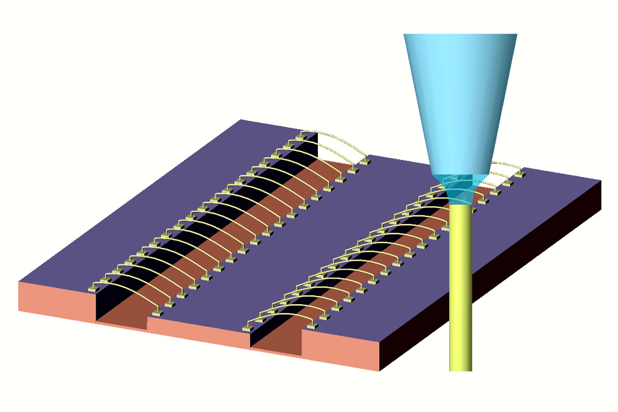
Engineers from the University of Illinois in the USA have developed an innovative method for the production of metallic connectors that could lead to the miniaturization of printed circuits and the advancement of the field of microelectronics

Engineers from the University of Illinois in the USA have developed an innovative method for the production of metallic connectors that could lead to the miniaturization of printed circuits and the advancement of the field of microelectronics.
Integrated circuits are produced by combining transistors and many electronic components together to obtain complex functions. The connections between chips and printed boards consist of metal wires prepared ahead of time and which are connected to the bonding area by the chip. "Combined functions require multiple wires. This type of wiring is tedious, time-consuming and expensive," said Min-Feng Yu, a professor of mechanical engineering at the University of Illinois.
In addition, this adhesion area occupies a large volume. As technology advances towards ever more miniaturized electronic components, the miniaturization of wiring becomes an increasingly significant obstacle. Many microelectronic devices are much smaller than the interconnect area of 50 square microns, a fact that prevents the development of integrated functions on such a tiny scale.
"Today there is no cost-effective method that allows wiring and integration of microstructures," said the lead researcher, "so let's get rid of these wires altogether, and instead why not produce them in the same place where they are needed between the connection points themselves?"
The researchers developed a direct production method for producing thin pure metal wires with a size that is much smaller than that found in normal wires and which require a connection area that is two orders of magnitude smaller. In an article published in the scientific journal Science, the researchers demonstrated how 20 innovative wires can be integrated into a single common connection area.
The new method will allow commercial companies to make pieces of semiconductor material that will contain many more chips per unit volume/area. In addition, it will allow more complex functions to be integrated into microelectronics components. The researchers demonstrated their method with both platinum and copper wires, and intend to test it for other metals as well.
The lead researcher compares his method to writing with a fountain pen. "People are used to drawing a vertical line on a two-dimensional surface, but what we do is write in three dimensions," he adds. The researchers filled a micropipette - a device capable of injecting tiny amounts of liquid - with an electrolyte solution containing copper. When the micropipette is brought very close to the surface, a liquid bridge forms between the pipette tip and the connecting piece. In the next step, the researchers activate an electric current that causes the copper in the solution to be deposited as a solid metal. As long as the tip moves against the surface, the copper continues and flows from the solution to the surface, in a similar way to the way ink flows from the pen, to obtain a copper wire. The big challenge for the researchers was to determine the appropriate moving speed of the pipette tip to maintain the acceptance of the liquid bridge between the nozzle and the "growing" thread.
"It is a liquid, so it can be shaped easily," explains the researcher. "As long as you keep the speed in the proper range, you can always produce uniform, high-quality wire."
In addition, the researchers had to find out how the wires can be "etched" transversely in order to connect chip to chip. The mouths of normal micropipettes are flat at their ends, but too high a tilt angle may "break" the liquid flow. The researchers discovered that a slotted nozzle, which has a ninety-degree cross section on its side, allows lateral movement - meaning that the wires can be made into an arched wire between one connection site and another, even if the chips are arranged in layers or stacks. The entire process is automated and the researchers hope to develop complete arrays of micropipettes to produce wire connections on an industrial scale.
"The advantage is that the work can be done in parallel," explains the researcher. "Instead of one fairy, imagine in your mind 10, 20 or even 100 fairies working at the same time. Dozens or hundreds of connections can be prepared in a single step, and this fact results in great financial savings." In addition to wire connections, the innovative method could lead to the development of many metallic microstructures for diverse applications.
"The ability to produce metallic three-dimensional structures in a simple and cheap way can pave the way for the development of many applications," notes the researcher.

2 תגובות
a question:
What happens when the copper is supposed to be solid at the top when there is a void underneath? How do you put it in the air?
Well done..
Very reminiscent of the XNUMXD printer.
Beautiful and useful. These are probably the last days in the field of miniaturization, which is almost reaching its limits.
What could perhaps move the entire field forward in a sharp change of angle is either quantum computing that simply requires fewer transistors, or wireless technologies for signal transitions - so that the chips will talk to each other without any wires at all.