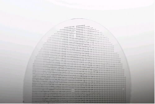
Researchers at Cornell have created perfect silicon surfaces in a test tube

Dr. Moshe Nahamani
Silicon is the "workhorse" of the electronics industry, and is used as the basic material for the development of tiny transistors that enable the operation of digital watches and computers. Now, scientists have succeeded in producing flat silicon layers with a thickness of almost a single atom, in the same structure used in the electronics industry, by a simple reaction at room temperature. These flat silicon layers can be used in the future for the development of biological and chemical sensors.
"In effect, we created perfect silicon surfaces in a test tube," says lead researcher Melissa Hines, a chemist at Cornell University. Researchers have already created perfect silicon surfaces in the past, but their previous work focused on silicon surfaces polished along the crystal plane that was not used in the electronics industry. The research group was able to produce flat surfaces along the crystal configuration used in industry today.
This discovery of the scientists is somewhat of a surprise. The researchers in the field believed that the melting process the team used to clean the silicon left the surfaces rough and bumpy. The lead researcher was writing a review paper at the same time and asked one of her students to photograph the resulting surface using a scanning tunneling microscope (STM) capable of simulating atomic-scale surfaces. "When we looked at the surface we unexpectedly realized that we were actually looking at an extremely flat surface," says the lead researcher.
The resulting microscope image showed a lined surface a single atom thick. Using additional measurement tools of computer simulations and infrared spectroscopy, the researchers determined that the silicon atoms in the row were connected at their ends to hydrogen atoms that would act as wax, which prevented the surface from reacting once it was exposed to air. "This means that if you take this flat surface, remove it from the aqueous solution and wash it from the reactants, it can be left in the air for 20-10 minutes without it starting to react," explains the lead researcher.
The researchers believe that one of the reasons their silicon surfaces remained so flat was that they dipped the surfaces into the solution and removed them from it every 15 seconds, which prevented the bubbles formed during the reaction from accumulating and causing uneven absorption.
At the same time, they also know thanks to the images from the STN microscope that helped them understand how flat the surfaces really were. "From an experimental point of view, the experiment is quite simple: you take a piece of silicon, mix it in a glass cup containing a solution, then take it out and look at it with the microscope. To be honest, there's no reason to believe that Bell Labs didn't create surfaces of our quality 20 years ago, but they didn't think to look at them with a microscope, so they didn't reveal it," notes the lead researcher.
The research team is currently working on adding different molecules to the flat silicon surface in hopes of developing new chemical and biological sensors.
The news about the study
