The development will accelerate applications in the nanotechnology industry * The results of the research were published in the prestigious journal Science

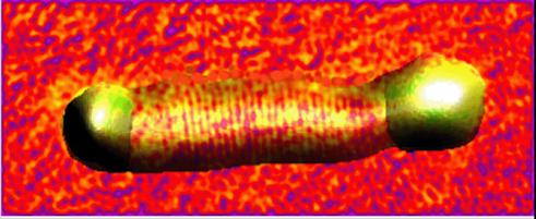
Researchers from the Center for Nanoscience and Nanotechnology at the Hebrew University of Jerusalem have developed nano-weights, that is, nano-crystals resembling small weights with a golden tip. (Nanocrystals are tiny particles a billionth of a meter in size, one hundred thousandth of the width of a hair). The application of the development in the future will be manifested in the creation of components such as nano-transistors and extremely tiny sensors based on these nano-crystals.
The nanocrystals are building blocks for innovative devices in nanotechnology, such as computer chips (tiny components), tiny nanosensors for chemical and biological substances, fluorescent markers in medical and biological applications, and more. A nanocrystal has unique electrical and optical properties, which can be controlled by changing the size of the particles, their shape or their composition.
The technology was developed in the research group of Professor Uri Benin from the Department of Physical Chemistry and the Center for Nanoscience and Nanotechnology at the Hebrew University and its results were published last Friday in the prestigious journal Science.
According to Prof. Uri Benin, "the revolutionary development of nanoweights may solve major problems that have so far prevented the commercial application of nanocrystals in a variety of fields."
"One of the challenges we face is connecting the nanocrystals to electric circuits. Such a connection must be extremely tiny and allow complex calculation operations to be performed simultaneously and in a few seconds. For example, in a Pentium 4 computer chip there are 40 million transistors, which allow it to perform complex operations at the same time and at enormous speed," explains Prof. Benin, "and in order to reach such complexity, a proper manufacturing process for the complex circuit is necessary. Another problem that must be overcome is improving the quality of the connection between the nanocrystal and the metal wire to ensure fast communication channels that will operate without faults."
The new technology developed by Prof. Benin and his research team offers a solution to both of these problems. In a simple chemical process, the researchers were able to achieve a selective growth of gold dots at the ends of the nanocrystals. The gold dots are connected by strong chemical bonds to the rod and the resulting nanostructure looks like a nanoweight. This structure will help in solving the problem of the contact of nanocrystals to electric circuits thanks to the tight contact.
It will also be possible to solve the problem of simultaneously connecting millions and billions of nanocrystals through 'self-organization' of the nanoweights, which results from the unique chemical properties of the gold edges.
The new discovery can be applied to a variety of semiconductor nanocrystals and will accelerate the integration of nanocrystals into real electrical circuits. "This discovery will bring us another big step closer to the commercial application of nanocrystals in a variety of fields," says Prof. Benin.
