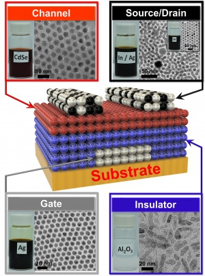
The innovative transistor consists of four types of ink: a conductor (silver), an insulator (aluminum oxide), a semiconductor (cadmium selenide) and a conductor in which an insulating material is integrated (a mixture of silver and indium).
[Translation by Dr. Nachmani Moshe]
The transistor is the most basic building block of the world of electronics, and is used to make electric circuits capable of amplifying electric signals or switching them between off/on states within a digital computing framework. The production of transistors is a very complex process, requiring special equipment suitable for conditions of high temperature and pressure. Now, engineers from the University of Pennsylvania have succeeded in demonstrating a new approach to making transistors and other electronic devices: placing layers of liquid nanocrystals on top of each other. Their research, which has just been published in the prestigious journal Science, paves the way for the development of electronic components that can be integrated into flexible or wearable applications, thanks to the fact that the process that takes place at a relatively low temperature is suitable for a wide variety of types of materials and can be applied in many fields.
The transistors based on nanocrystals were printed on a flexible plastic substrate using a spin coating method, although in the future it will be possible to produce them using a simpler method, for example XNUMXD printing. The first step was taking nanocrystals, or spherical nanoscale particles that have the electronic properties required for a transistor and putting them into a liquid, creating an ink composed of nanocrystals. The researchers created a collection of four types of ink: a conductor (silver), an insulator (aluminum oxide), a semi-conductor (cadmium selenide) and a conductor in which an insulating material (a mixture of silver and indium) is incorporated. The "plating" of the semi-conducting layer of the transistor with another material allows control over the way in which the device transfers a positive or negative charge.
"The materials we developed are exactly like the ink used in the commercial injection printer found in every home or office today," explains the lead researcher. "However, our materials can be easily modified so that each of them can function as a conductor, semiconductor or insulator. Our research question was whether it is possible to stack them on top of each other on a surface in such a way as to allow them to function together to obtain an active transistor." The electronic properties of some of these ink types have been verified separately in the past, but they have never been combined together to obtain a complete device. "This is the first work ever showing that all the components, metallic, insulating and semi-conducting, of the transistor can be used together to make nanocrystals."
In the first step, the ink of the electrically conductive silver nanocrystals is placed on a flexible plastic surface previously treated with a photolithographic mask and then quickly removed to obtain a uniform layer in thickness in the shape of the gate electrode of the transistor. In the following steps, the researchers placed another layer of insulator, a semi-conductor and in the last step the drilled layer. With the help of moderate heating at a low temperature, the solidified material is blown out of its original layer into the semi-conducting layer. "The important factor in working with substances in solution lies in the fact that we make sure that when the second layer is added, it does not wash out the first, and so on," explains the lead researcher. "We have to make sure that the layers really adhere to each other without interfering with each other." In view of the fact that this entire production process, based on an ink solution, takes place at low temperatures and not under vacuum conditions, as is customary today, the researchers were able to place several transistors on the same flexible plastic surface at the same time.

5 תגובות
Small correction: as mentioned, the behavior of a flash device is considered classical behavior, but during its charging with electrons (="writing"), both classical movement and tunneling of the electrons through the insulating barrier on the silicon surface are considered.
Yossi, Intel worldwide also refers to its 22 and 14 nm chips in a classical and non-quantum way, even though their behavior is undoubtedly quantum. The same goes for all disk-on-key devices today, which are also strictly quantum (each "cell" in a standard flash chip stores less than 1,000 electrons for up to 7 years). It's just more convenient to work assuming classic behavior.
It turns out that the same MOS (transistor with oxide) principles are used in these as well, although if we ask a physicist - this is not the correct description.
https://arxiv.org/ftp/cond-mat/papers/9710/9710326.pdf
The laws of conduction change in such dimensions from classical to quantum. A standard MOSFET transistor is shown here.
What are the dimensions of the transistor?