Scientists from the Georgia Institute of Technology have developed a nanolithography method capable of producing arrays of three different chemicals, at a high level of separation, within a single chip

Scientists from the Georgia Institute of Technology have developed a nanolithography method capable of producing arrays of three different chemicals, at a high level of separation, within a single chip, at an injection speed of up to one millimeter per second. The chemical nanoarrays can then be shaped at will into any shape and structure and are stable enough to be stored for weeks and used later elsewhere.
The method, known as "Thermochemical Nanolithography", is fully described in the scientific journal Advanced Functional Materials. The research could have possible applications in several scientific fields ranging from electronics to medicine.
"The power of this method lies in its ability to embed chemical templates in a cheap, compact and high separation capacity on samples, which can be transferred to any laboratory around the world, and then immerse the samples in any desired solution for the preparation of nanostructures with proteins, DNA. or nanoparticles," said researcher Elisa Riedo, a professor in the School of Physics at the Georgia Institute of Technology.
Conceptually, the method is surprising in its simplicity. Using an atomic force microscope (AFM), the researchers heat a silicon tip and move it over a thin polymer layer. The heat released from the tip induces a local chemical reaction on the thin surface. This reaction changes the chemical nature of the surface and turns it from an inert surface to an active one, one that is capable of selectively binding these chemical separations. The research team first developed the method in 2007. Now, they have added several new improvements to it that could make the method an extremely useful tool for scientists working at the nanometer level.
"We have created a method for imprinting independent patterns of several different chemicals on a chip that can be shaped in any shape we want," says one of the research partners.
The ability to make high-resolution items of different chemicals in diverse forms is important since some nanolithographic methods are limited to only one type of chemistry, low resolutions, or defined structures. In addition, the work rate of the new method, of one millimeter per second, is several orders of magnitude higher than existing lithography methods where the rate is about 0.0001 millimeter per second for each "writing" tip.
The research was made possible thanks to heated AFM detector tips capable of producing hot spots with a tiny diameter of a few nanometers. "The heated tip allows scientists to direct chemical reactions at the nanometer level," says the lead researcher.
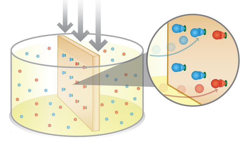
With the new method, multiple chemical patterns can be obtained on the same chip by using the AFM tip to heat the polymer layer and change its activity level. In the next step, the chip is dipped in a solution that allows the chemicals (such as proteins or other chemical binders) within it to bind to the chip at those preheated points. The AFM tip then heats additional spots and again other chemicals can be attached to them.
In their paper, the scientists demonstrated how amines, thiols, aldehydes and biotin can be attached using this method. Basically, this method can be used for the binding of any chemical. In their research, the scientists also demonstrate how the chemical patterns are used to organize functional materials on the surface, materials such as proteins and DNA sequences.
"The great advantage of this method lies in the fact that it works with almost any chemical substance or chemically active nanoparticle. It allows scientists to very quickly connect different and diverse components that can, afterwards, be converted into more complex and different structures, which in turn can be selectively attached to other items (electrodes, sensors, etc.). So it doesn't matter if you are interested in biology, electronics, medicine or chemistry, the method allows you to create any desired chemical pattern," says one of the researchers. In addition, the stability of the method allows its use even in the hands of scientists who are not specifically experts in the field of fine nanolithography.
"From the moment you stamped the pattern, it is stable and inactive. We showed that it can be preserved for over a month, then dipped in a solution and still become active again, at the moment we want," explains the lead researcher.
