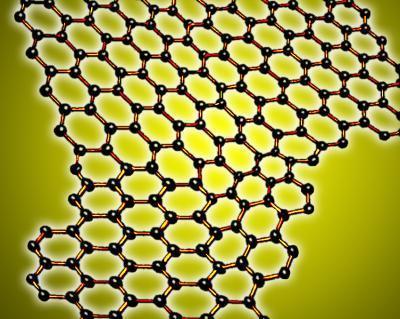
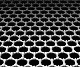
Graphene is a two-dimensional crystalline form of carbon: a single layer of carbon atoms arranged in a hexagonal structure, similar to wire with a hexagonal mesh. As independent objects, no one believed they could be manufactured - or even existed - until physicists at the University of Manchester were able to actually manufacture them in 2004. Now this material is being targeted for an important role in accelerating computing.

Researchers in the Department of Advanced Energy Sources (ALS), from the National Laboratory at the University of California, San Diego (UCSD), have now been able to measure unusual properties of graphene with a level of precision never before achieved. The results confirm many of the strange properties of this unusual material, but also reveal significant deviations from theoretical predictions about it. They also point the way to its practical applications, such as tunable optical modulators for the fields of communications and nanoelectronics.
Promising electronic properties of graphene
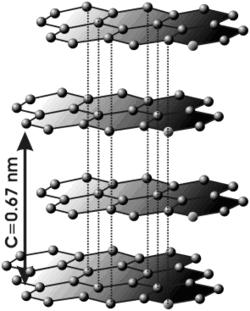
The form of carbon known from pencils, graphite, is built of layers containing rings with six carbons (hexagonal) in a way where each carbon is connected to three other carbons by strong bonds (covalents). The layers are far from each other and connected by loose bonds (van der Waals), which makes graphite soft. Between the layers are mobile electrons (the fourth non-bonding electron in the shell of each carbon atom) and enable electrical conductivity. Since the layers are able to move easily over each other, graphite is an excellent lubricant.
In the same subject: a new formation method
In fact, these graphite layers are the graphene, although before 2004 they were not observed in isolation. Once its existence was confirmed, researchers began an extensive research race, encouraged by the unexpected electronic properties of the new material. The studies began and have continued since then without respite. "The special electronic properties of graphene are due to the fact that the carbon atom has four electrons, three of which are bonded to each other," says the researcher. "But the fourth non-bonded electron is found in orbitals that extend perpendicular to the plane, above and below it, and their hybridization spreads over the entire surface of the graphene." Being a crystal, XNUMXD graphene is very different from XNUMXD materials such as Zorn.
In semiconductors and other materials, electric charge carriers (electrons and their opposite "holes") react with the periodic field of the atomic lattice to obtain "quasiparticles", an extension that behaves like actual particles. But this situation in graphene is not at all similar to its counterpart in typical semiconductors. The energies of these particle-like particles in the solid depend on their momentum, a relationship described by means of energy bands. In a typical three-dimensional semiconductor, the energy bands are "parabolic" - a curve in which there is a full valence band at the bottom (in a shape similar to a planar stalagmite, more or less, at the peak), while at the top there is an opposite empty conduction band (in the form which resembles a planar stalactite, more or less at the bottom); and between them an empty band gap, which represents the amount of energy required to move an electron from the valence band to the conduction band.

However, unlike typical semiconductors, the valence band and conduction band curves in graphene resemble smooth cones with their sides intersecting at one point, known as the "Dirac point". These describe the momentum-energy ratio of the particle-like particles as if they behaved as massless electrons, particles called "Dirac fermions", moving at a constant speed, less than the speed of light. One interesting result of this special energy band structure in graphene is the fact that the electrons in it are quite free, says the lead researcher. Unlike electrons in other materials, the electrons in graphene "move" ballistically - without any collisions - through large distances, even at room temperature. As a result, the ability of the electrons in graphene to conduct an electric current is ten to a hundred times higher than in other typical semiconductors, such as silicon. This fact makes graphene a very promising candidate for future electronic applications. "By applying a current through graphene inserted into an electrical device, it is possible to continuously control the density of the charge carriers by changing the applied current, and hence control the conductivity," says lead researcher Lee. This is the unique feature that enables promising applications using graphene.
An extraordinary experiment
Since it is very difficult to produce graphene and even more so to treat it, most of the experiments were carried out not on the free surfaces themselves but on two types of graphene samples: "exfoliated graphene", which is "glued" to zinc oxide/zinc substrate, and epitaxial graphene , a layer of carbon atoms chemically bound to a suitable substrate of silicon carbide. "These two types of graphene surfaces are essentially different," the researcher tells me. Most of the experimental research in a particle accelerator on epitaxial graphene used a technique known as ARPES, angle-resolved photoemission spectroscopy. "In our study, the experiments were performed on glued graphene using infrared spectral microscopy."

The researcher explains that measurements at infrared wavelengths can test the dynamic properties of quasi-particles over a wide range of energies, and hence - can provide some of the most intriguing information regarding the electronic nature of materials, such as the lifetime of the electrons and their interactions. "Such measurements have not previously been performed on glued graphene, because it is very difficult to measure the absorption of light in a single layer of graphene." In order to accurately measure the behavior of the graphene in response to infrared radiation and in relation to changes in the current applied to it, the researchers needed glued graphene samples that were connected to the electrodes. They used flakes of atomic monolayers of graphene measuring 50 square micrometers. The samples were placed over (without chemical bonding) an isolated layer of zinc oxide and another layer of pure zinc. This transparent substrate is used as a gate electrode. The whole system was cooled to 45 degrees Kelvin.
"In order to measure the absorption of the infrared beam using natural graphene and graphene placed electrostatically, that is, not chemically bound, like the one present in the electrode, we required the intensity and focus of radiation from a particle accelerator at infrared wavelengths," says Michael Martin, one of the researchers. "The beam, which was no more than ten micrometers in diameter, was aimed at different points along the length and width of the sample, thus allowing us to directly measure the optical conductivity of the material." The word "optical" in the concept of "optical conductivity" refers to the high frequency of light, as opposed to the very low frequency of household alternating current (AC). The researchers created alternating electrical induction at the optical frequency of the graphene samples using the infrared beam and changed the voltage through the electrodes. These changes in voltage resulted in changes in the conductivity and density of the electric charge carriers in the samples, and directly affected the reflection and absorption of light.
In doing so, the researchers showed that the electronic properties of graphene can be adjusted in a controlled manner. "In a typical semiconductor electronic system, the 'Fermi energy' - the energy of the charge carriers in the highest occupied quantum state at absolute zero - is a function of the carrier density," Lee says. "However, in systems of two-dimensional Dirac fermions, Fermi energy is a function of the square root of the carrier density." The researchers did observe the square root dependence of this unique density on the Fermi energy, and hence proved that the electrons in graphene do indeed behave as Dirac fermions. The researchers predicted this square root dependence of the Fermi energy on the carrier density, and hence confirmed the assumption that the electrons in graphene indeed behave as Dirac fermions. Therefore, many of the properties of graphene predicted by theory were confirmed in these experiments, and were measured with a level of precision that had not been achieved before.
Surprises in graphene
Other results, however, revealed a more complex behavior of "many-body interactions" than that suggested by the image of graphene as a single object, which treats the charge carriers as a collection of independent particles . The theory predicted that if the electrons in graphene do not have any interactions with each other or with the carbon atom, then at low energy (or frequency) - energy less than twice the Fermi energy - they will barely absorb any light. Instead, the researchers predicted significant absorption of infrared radiation in this low-energy region. "This unexpected absorption originates, possibly, from the interactions between the electrons and the general vibration of the carbon atoms of the crystal lattice, or from the interactions between the electrons themselves," says the lead researcher.
Another surprising result is the speed of electrons. Being free particles, the electrons in graphene should move at a constant speed regardless of their energy. However, the researchers found that at high energies the electrons do move at a constant speed, but their speed systematically increases as their energy is reduced. This mysterious behavior lies, perhaps, in the interactions between the electrons themselves as predicted theoretically back in 1994. "The interactions of many particles can be depicted as simple Coulomb interactions between electrons, or they can be more complex," says Martin. "The information collected gives a clear pattern, but we still don't fully understand it." "Some of these phenomena can be related to the limitations of the graphene samples we used," says Lee. "We were very interested in performing these measurements on pure graphene samples to avoid any side effect of the substrate. And yet, despite these possible deviations, it seems that our measurements pose a challenge in the current understanding of this fascinating material."

5 תגובות
The processing power of an electronic processor increases as the electrons inside it can move faster?
Very nice but a problem with the interpretations. While most of the terms are explained, the terms stalagmite and stalactite are given as an explanation for the structure of the stripes, but are even less familiar to Hebrew readers who are not geologists. That is, this explanation is effective only for geologists, or for those who know solid state physics, but not for the rest.
Simply writing stalactite instead of stalagmite and sentinel instead of stalactite would be more helpful.
All these "strange" phenomena result from the disruption of the glue (which sticks to the substrate) the structure of the lattice
Fascinating..worth concentration.