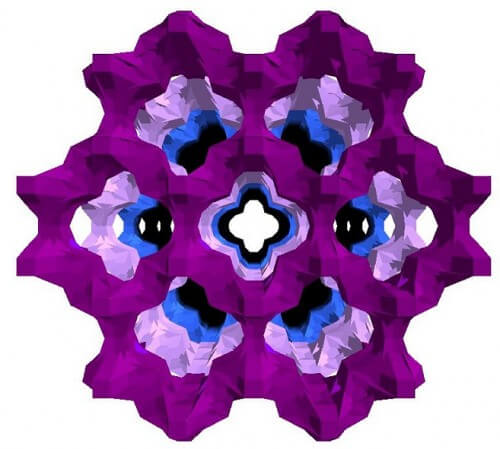
A completely new form of viewing structures at the nanometer level has been developed at the German Johannes Gutenberg University

A completely new form of viewing structures at the nanometer level has been developed at the German Johannes Gutenberg University. This method enables the precise determination of the spatial arrangement of the atoms and molecules within a variety of materials, from cement to medicines. The method is based on electron microscopy and allows observation of the smallest crystals.
The arrangement of atoms and molecules in a solid has a decisive effect on the physical properties of the material. Structures such as these were examined for the first time in 1895 using X-rays, a method that has since become a daily procedure. The beginning of research in this field included the discovery in 1912 that crystals are composed of small lattices - a characteristic responsible for the variety of thermal, electrical, visual and mechanical properties inherent in these materials. "The fact that this method still has an impact on our understanding of solids and their properties is reflected in the number of Nobel laureates who won the prize based on structural analyses," the researcher notes.
In the age of nanotechnology, however, science focuses more and more on very tiny particles, which can no longer be observed through structural analysis based on X-rays. For example, structural analysis using X-rays of a single crystal is only possible up to a crystal size of about one micrometer, i.e. - a thousandth of a millimeter. Below this threshold, it is necessary to use other methods, such as electron diffraction tomography (EDT) or automated diffraction tomography (ADT), which allow to produce structural images of individual crystals for the first time ever. "It's like we turned a spotlight on the world of nanostructures," gushes the lead researcher. Similar to electron microscopy, the method is generally based on the idea of an electron beam directed towards an object and being reflected from it. The electron diffraction pattern allows determining the position of the atoms within the structure.
During the last decade, Dr. Kolb's research group developed electron diffraction tomography of a single crystal. Their first success was in 2009 with the determination of the structure of barium sulfate. "Since then, the number of materials whose structure we have been able to decipher has become enormous," adds the researcher. The most recent example is the determination of the structure of the ITQ-43 zeolite in collaboration with Spanish and Chinese scientists. Zeolites are crystals consisting of a compound of clay and silicate. They have tiny pores that make them particularly important in the field of energy and environmental technologies thanks to their potential to be used as adsorbents, ion exchangers and catalysts. In the field of water treatment, zeolites help remove heavy metals; In the oil and gas industry, their application was like a micro-revolution in the cracking process of crude oil. We also encounter them in everyday life, for example, as an ingredient in washing powders. A team of scientists from the Technical University of Valencia prepared a zeolite with small and medium-sized pores, the combination of which gives rise to a funnel-like zeolite, a characteristic that further increases their catalytic activity. In an article recently published in the prestigious scientific journal Science, the researchers describe how they determined the complex crystal structure of this material using the ADT method.
"The smaller the size of the zeolite crystals, the greater their catalytic efficiency," explains the researcher. For crystals with a size of about one hundred nanometers, the mechanized tomographic method is sometimes the only method that allows a complete and accurate observation of the internal structure. "There are a large number of solid materials, both natural and synthetic, for which our method can be useful - materials that are not available or cannot be produced in a suitable crystal size." Thus, for the past two years, a wide variety of materials have passed under Dr. Kolb's microscope, starting with pigments and metal oxides used in solar energy technologies, and ending with precious minerals.
Compared to normal electron microscopy, electron diffraction tomography is much faster, as well as more accurate and complete. While the structures of the materials used to be determined over two whole years, the results of the new method are obtained in just one day. Even materials that are sensitive to a radiation beam can, in principle, be suitable for this method, which is described by the main researcher as "computed tomography (CT) of crystals".
The method shares an important feature with computed tomography which is an important part of its success: the test sample that is under the microscope undergoes a gradual area scan using an extremely tiny tip in order to collect information from a wide variety of varying angles. By exploiting this trick, the scientists can avoid the main problem in this field: the strong interactions between the electron beam and the sample have made electron diffraction, until now, more complicated.
A video demonstrating the method
