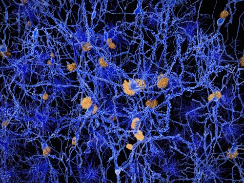
The platform, which consists of silicon, silicon dioxide and metal, will be able to improve the resolution of microscopes and will allow imaging of both intracellular processes and of a single transistor during production. "Focusing light to such dimensions has already been achieved in the past with visible light, but only with the help of complex patterns such as nanoantennas
Researchers at the Technion have developed a technology for compressing light waves in a way that makes it possible to focus the light into a beam with nanometer dimensions. Medical and biological imaging, nanolithography (printing tiny electronic components) and "lab on a chip" applications - these are some of the applied fields whose development depends on precise focusing of light. The problem is that the focusing of light into tiny dots, which are tens of nanometers in size, is limited by the "diffraction limit" - a term coined by the German physicist Ernst Carl Abe. Abe discovered that the focus of light (in a light beam) and the resolution of a microscope are limited to half the wavelength of light.
From the definition of the "diffraction limit" it follows that the more we decrease the wavelength, the higher the resolution we will get. Now, a group of researchers led by Prof. Guy Bartel from the Faculty of Electrical Engineering at the Technion has developed a new platform that "compresses the wave" and shortens it to a quarter of its length without changing its frequency (the "color"). In other words, Prof. Bartel and his colleagues managed to "push" the limit of diffraction (diffraction) by shortening the wavelength.
The platform, which consists of silicon, silicon dioxide and metal, will be able to improve the resolution of microscopes and will allow imaging of both intracellular processes and of a single transistor during production. "Focusing light to such dimensions has already been achieved in the past with visible light, but only with the help of complex patterns such as nanoantennas," explains Prof. Bartel. "Now, with our platform, it will be possible to promote applications in medical imaging and the production of electronic components."
"By means of a resolution that matches the new technological needs, and while preserving the simplicity and flexibility of diffraction-limited systems, we are paving the way for the development of a simple and easy-to-manufacture microscopy tool suitable for the needs of the semiconductor industry," explained Dr. Bergin Jiunai, a senior researcher in the laboratory of Prof. Bartel Asher developed a method for dynamic control of the position of the nanometer light beam.
One of the breakthroughs in the field of super-resolution won its developers the Nobel Prize in Chemistry for 2014. Professors Eric Betzig, William Morner and Stefan Hell developed 'nanoscopy' - high-resolution fluorescence microscopy. This step led the optical microscope to the nanometer era and today makes it possible to see biological activities at the molecular level, by 'bypassing' the diffraction limit. "The problem is that the current devices that realize the same theoretical breakthrough are still bulky, slow, expensive and energy-hungry," says Prof. Bartel. "My goal is to promote the realization of those discoveries with more efficient devices. The current article presents a characterization of the system, and the next step is the proof of feasibility."
Prof. Bartel deals with nano-optics and examines how light and waves progress in structures whose size is smaller than the wavelength. This requires a new type of artificially engineered materials that incorporate metals and insulators. He investigates special wave phenomena and their applications in such materials, which make it possible to conduct and manipulate waves in a way that is not possible in natural materials. This field - Plasmonics and Metamaterials - presents an innovative approach to routing waves in dimensions smaller than the wavelength, while overcoming the diffraction limit. The research is experimental and theoretical, and includes microelectronics and nanoelectronics facilities for making models (fabrication), a pulsed laser and a near-field microscope for characterization, theory and simulation needs.
The research was partially funded by the KLA-Tencor company and the National Science Foundation (ISF) and will be presented at the Nano Israel 2016 conference, which will be held this week at Tel Aviv University.
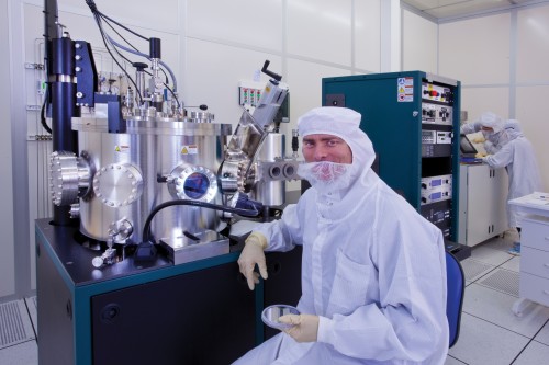
Prof. Guy Bartel. Photo: Technion spokespeople

9 תגובות
Thanks Nissim.
Joseph
Yes - if the refractive index is 4 then both the speed and the wavelength are 4 times smaller.
Besides, the professor studies apparently one-dimensional quantum structures. That is, in the direction of the growth of the crystal the quantum dimensions, in other directions not necessarily. Growing the crystal layers looks like spreading layers of chocolate, jam, butter between 2 sandwiches. That is, the material has patterns of absorption of a rectangular pit of energy, because of the energy gaps in the electron conduction band and the valence band. That is, light can apparently be trapped at certain frequencies. If the structure is cyclic then apart from the pits, a lattice is apparently formed and then a new valence band and a new conduction band are formed - and the decay of excited electrons is among possible energetic bands of existence. New engineered material. All this I emphasize is a speculative guess as far as I'm concerned and I need to read the original material a bit - sounds interesting - still the article is informative, you need to read to see the innovative mechanism.
Miracles.
A refractive index greater than one means a slower c/N propagation speed. If I understood what you explained to Yehuda: apparently the wavelength is shortened N times: if the cycle time is T then the wavelength is the way cT/N. Is that the explanation? Gently, like Judas.
Yehuda
The refractive index of glass can be 3, and there are materials with a refractive index close to 40.
How to move at a wavelength smaller than the speed of light in matter. Neta's question interests me too. Light reacts with matter, but I haven't heard that matter seems to speed up light. I heard he was slowing down.
Yehuda: Indeed. If light does not move in a vacuum, there is no law that requires it to move "at the speed of light" (the famous Snell's law is due to different speeds of light in different mediums).
Breaking the diffraction limit is a huge achievement that breaks conventions. What about the *explanation* of the theoretical or technological idea?
The article reads: "Prof. Guy Bartel from the Faculty of Electrical Engineering at the Technion has developed a new platform that "compresses the wave" and shortens it to a quarter of its length without changing its frequency (the "color"). In other words, Prof. Bartel and his colleagues managed to "push" the limit of diffraction (diffraction) by shortening the wavelength." End quote.
If the wavelength is shortened to a quarter without changing the frequency, does it follow that they succeeded in reducing the speed of light to 75,000 km per second?
Please respond gently
Yehuda