Ibhas developed a process for silicon recycling of old electronic chips, and converting it to use in solar panels - dedicated panels in solar collectors that produce clean electrical energy
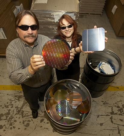
In the picture: a new unique IBM process turns an abnormal silicon wafer (left) into a solar panel that enables the production of electricity from the sun's rays (right).
IBM has developed a process for silicon recycling of old electronic chips, and converting it to use in solar panels - dedicated panels in solar collectors that produce clean electrical energy.
The silicon wafers used by IBM to manufacture chips for the computer and cell phone industry find new life in the form of solar cells. A team of developers at the IBM manufacturing site in Burlington, USA, has developed an innovative process that uses the remains of silicon wafers to produce solar panels - while saving money, reducing the amount of waste, protecting the environment, and helping to expand the solar energy industry.
BMW estimates that approximately three million wafers of silicon are thrown into the trash every year in the factories of the microelectronics industry, after their production processes were not precise enough. These three million slices are able to cover a land area of about 80 dunams - which, if turned into solar collectors, could produce 13.5 megawatts of electricity (57 million kilowatts/hour of solar panels, based on an average of 12 hours of light a day, 365 days a year). This amount of energy covers the average consumption of about 6,000 homes per year.
IBM uses the silicon wafers, less than a millimeter thick and 24 to 30 cm in diameter, to manufacture chips at its microelectronics factories in Burlington and East Fishkill. The manufacturing process includes light-embossing of tiny wiring, which turns each wafer into a large number of chips for various purposes: from cell phones and consumer electronics to super servers.
The manufacturing process of silicon chips requires the use of several such smooth wafers as a "monitor": control components for the purpose of performing tests and supervising the process. The use of each such control slice is limited to a limited number of times - before the slice is no longer able to fulfill this purpose. Now, IBM is offering these wafers for sale to manufacturers in the solar panel industry, who need the same silicon materials to make photovoltaic cells.
The timing in which IBM enters the solar energy market is particularly good, in view of the apparent increase in demand for solar panels - while the supply of raw materials lags behind its growth rates.
The IBM development team further expanded and increased the savings in raw materials, through the development of a unique and environmentally friendly process, in which silicon wafers where faults are detected in the production processes are turned into control wafers. These wafers are polished with water and an absorbent pad, to remove the conductor layer that was embedded on them, return to the production line as control wafers, and leave it for the last time to be sent to solar panel manufacturers. The development of the process was done within the framework of IBM's overall environmental commitment, which strives to reduce pollution, reuse and recycling in its production processes. Along the way, it saves the purchase of silicon for dedicated control wafers - and provides raw materials for the solar energy industry, which also helps preserve and improve the quality of the environment.

6 תגובות
thanks Michael
Billy:
You have an error in the factor of 10 because it comes out to be 13.3333 but the truth is that this should not be enough for the electricity consumption of a housing unit either.
According to a calculation of 80 dunams for 6000 housing units, a total of 1.3 square meters per housing unit, right? Someone correct me
There has been a cycle method for several years...
Even if it's a negligible amount, I'm glad that one of the biggest players in the technology world is giving it some thought. Oil may run out in not many years, and solar energy
It is the second best option (along with nuclear energy).
Ran
Listen to my programs 'Making History', podcast
Bi-weekly on the history of science and technology.
The program was rated five stars on the website
icast.co.il and over a thousand listenings.
The program's homepage
http://www.ranlevi.blogspot.com
80 dunams per year if all the silicon wafers are used. This is a negligible percentage of the total solar cell industry.
A nice invention but mostly good for public relations.