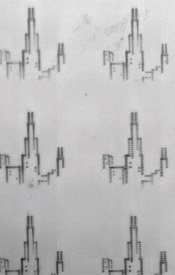
A research team from Northwestern University (NU) was able to draw 15,000 identical painting patterns using tiny beams of light thanks to an innovative nanomanufacturing method known as "pen-beam lithography"

A research team from Northwestern University (NU) was able to draw 15,000 identical painting patterns using tiny beams of light thanks to an innovative nanomanufacturing method known as "beam-pen lithography" (BPL).
The innovative method provides a fast and economical means for the design and preparation of electrical circuits, opto-electronics components and devices for medical diagnosis and contains many other applications in the field of electronics, photonics and the life sciences industries. Details about the new method were published in the scientific journal Nature Nanotechnology.
"It's all about miniaturization," said Chad A. Mirkin, professor of chemistry and head of the university's International Nanotechnology Institute. "The rapid transfer of large volumes of information drives the world today. However, conventional nano- and micro-fabrication means are extremely expensive. We are trying to overcome this obstacle through a new approach to photolithography and nanodesign.”
Using pen-beam lithography, the researchers were able to draw 15,000 replicas of the Chicago skyline simultaneously in half an hour. 15,000 tiny pens drew the skylines on a square centimeter of space. Conventional nanodesign methods, such as electron beam lithography, do allow the production of such tiny structures, but their output is small and they do not allow large-scale nanoproduction.
Each skyline pattern consists of 182 dots, with each dot having a diameter of 500 nanometers, similar to the diameter of a pen tip. The projection time of each point was 20 seconds. This method allows the researchers to produce tiny structures as small as 150 nanometers, but improvements in the pen structure could likely increase the resolution down to a hundred nanometers or less. Although this finding was not reported in the article, the researchers were able to create an array of 11 million pens using a piece the size of only a few cm.
A beam pen is the third type of "pen" in Mirkin's collection of nanoproduction tools. He developed polymer-pen lithography (PPL) in 2008 and dip-pen nanolithography (DPN) in 1999, both of which are used to transfer chemicals to a surface and have since been commercialized and are used as nanomanufacturing tools commonly used today in 23 countries around the world.
Similar to the PPL method, pen-beam lithography uses an array of tiny pens made up of polymer to "print" patterns on large surfaces at a nanometer to macroscopic level of separation. However, instead of using the "ink" of furods, the method draws patterns using light through a light-sensitive material.
Each pen is designed in the shape of a pyramid with the top of the pyramid serving as a nib. The researchers coated the entire pyramid with a thin layer of gold and then removed a small amount of gold from the tip. The wide open base of the pyramid (the other end of the structure) is exposed to light, and the gold-covered pyramid directs the radiation towards the tip. From this point a narrow beam of light is emitted which exposes the radiation-sensitive material at each and every point of it. This allows researchers to draw patterns easily and with great accuracy.
"Another advantage is that it is not necessary to use all the pens at once - we can "turn off" some of them and "turn on" others," explained the researcher. "Since the heads of the pyramids are micron in size, each and every one of them can be controlled individually."
"The method will advance the development of devices that will enable researchers in universities and the electronics industry around the world to rapidly design a prototype - and perhaps even produce - electronic devices and systems with high resolution directly in the laboratory," said the lead researcher. "Researchers are interested in testing the activity of their template immediately and not waiting for its prototype to be produced by a third party, which is the current situation."

2 תגובות
These are not 182 points arranged in a straight line. The whole drawing is about 182 points arranged in the shape of the skyline.
"Each pattern of the skyline consists of 182 points, with each point having a diameter of 500 nanometers, similar to the diameter of the nib of a pen. The projection time of each point was 20 seconds. This method allows researchers to produce tiny structures with a size of 150 nanometers"
Something in the calculation doesn't quite work out for me... 182 points where each one is half a micron means that the total length of this is 91 microns. With 15 thousand of these we reached almost one and a half cm and that's just the size of the painting. According to the picture it also has volume and there is a distance between the drawings and these are much larger than the area of the line itself. I don't see how this operation sits on one square centimeter.
Greetings friends,
Ami Bachar