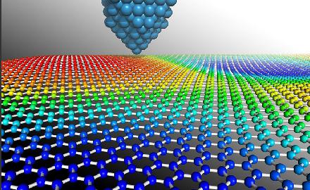
The method developed at the Georgia Institute of Technology may facilitate the production of nanowires that will conduct electricity in graphene-based electronics

A simple one-step process, producing both p- and n-type plating of extensive graphene surfaces, could advance the use of this promising material for future electronic devices. The innovative plating method could also be used to increase electrical conductivity in graphene nanostrips used in computer connections.
By combining a commercially available spin-on-glass (SOG) material with graphene and exposing them to electron beam radiation, the researchers from the Georgia Institute of Technology, USA, were able to create both types of plating simply by Changing the exposure time of the beam - high levels of irradiation give rise to p-type complexes, while low levels give rise to n-type complexes.
The method was used to prepare high quality pn junctions. If the researchers succeed in making the metal less chemically active, they expect that the conductivity created in the graphene sheets will remain constant.
"This is a step that could advance the possible preparation of graphene-based transistors and complementary metal oxides," notes one of the researchers. The research findings were published in the scientific journal Applied Physics Letters.
The innovative plating process begins when the researchers remove flakes of graphene, one to four layers thick each, from a block of graphite. They place the layers on a surface of oxidized tin and operate a suitable contact device on the system.
Next, they spin spin layers of the photosensitive material hydrogen silsesquoxane (HSQ) and then fix certain parts of the resulting thin layer using electron beam radiation. The method provides precise control over the amount of radiation and the precise points in the graphene on which it is applied, along with higher levels of energy, obtained from increased crosslinking of the HSQ material.
"We activated varying levels of electron radiation and then examined their effect on the properties of the charge carriers in the graphene lattice," explains one of the researchers. "The electron beam provided us with a sharp range of control that is invaluable for the production of nanometer devices. We are able to operate an electron beam with a diameter of only four or five nanometers, which allows us to obtain very precise plating patterns."
The researchers point out that electrical measurements showed that the pn junction in graphene, created by the new method, has a high energy separation - a fact that indicates strong conduction effects. Researchers in other laboratories around the world have demonstrated the deposition of graphene in a variety of processes, including immersing the material in various solutions and exposing it to a variety of gases. The new process is the first that allows electron plating and hole plating in the same material.
The researchers point out that graphene plating processes are supposed to be very different from those used today to plate Zorn. For Zoran, in the plating phase, atoms of the Zoran lattice are converted into atoms of another material. In the new one-step process for splicing graphene, the researchers believe that splicing allows the introduction of hydrogen and oxygen atoms near the carbon lattice. The hydrogen and oxygen atoms do not convert the carbon atoms, but they occupy places above the lattice structure.
"Energy supplied to the spin glass breaks chemical bonds and releases hydrogen and oxygen atoms that bind instead to the carbon lattice," explains one of the researchers. "Strong electron energy changes the entire structure of the spin glass into a kind of network, and then more oxygen atoms than hydrogen are formed and thus an n-type doping is obtained."
In more mass production, it is likely that electron beam radiation will be replaced by normal lithography processes, explains the researcher. A change in the degree of reflection (reflectance) or the degree of transmission (transmission) of the mask set will result in control of the amount of radiation that reaches the spin glass, and this will determine, in the end, whether n-type or p-type regions will be produced.
"Making all the moves in one step will lead to avoiding some of the expensive lithography steps," he says. "Gray-scale lithography will enable precise control of the plating along the entire length of the chip surface."
To plate large areas as junctions, which do not require inserting templates into them, the researchers will simply cover them with the HSQ material and expose them to the plasma source. The method is able to increase the conductivity of the nanostrips up to ten times more than untreated graphene.
Since the HSQ material is already well known to the microelectronics industry, the one-step approach could help adapt graphene to existing processes, while avoiding a change in semiconductor processing and manufacturing systems. The researchers intend to better understand how exactly the process occurs and whether other polymers will lead to improved performance.

2 תגובות
we will remember
The next generation of solar energy harvesting begins with this process. Remember my words.