A technology developed at the Technion may replace silicon chips in the world of electronics. The development is published in the journal Nature Communications
Since their discovery, CNTs (tiny carbon tubes) have aroused great interest in the scientific community due to their unique properties in aspects such as electrical conduction, optics, heat, mechanical properties and sensitivity to chemical substances. These tubes are considered a significant component in the electronics of the future. Recently an entire computer based on them was introduced, and it is possible that in the future they will be able to replace the silicon chip as the building block of electronics.
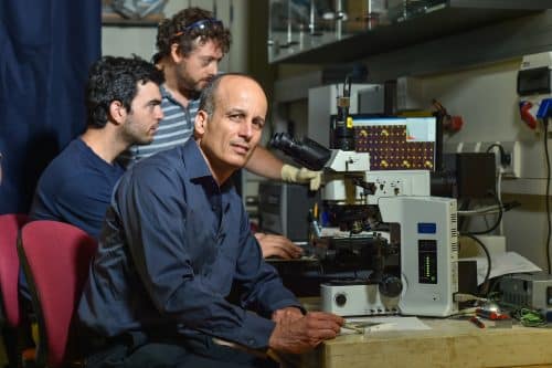
One of the biggest challenges on the way to the application of CNTs is related to the need to produce them in specific locations on a smooth substrate, under conditions that will lead to the formation of an electric circuit around them. An article published in the journal Nature Communications presents a breakthrough in this matter, achieved in the laboratory of Prof. Yuval Yaish from the Viterbi Faculty of Electrical Engineering and the Zisafel Center for Nanoelectronics at the Technion. The technology developed by Prof. Ya'ish, which produces the aforementioned conditions, and furthermore, also allows to study the dynamic properties of the carbon tubes, including acceleration, resonance (vibration) and the transition from softness to hardness.
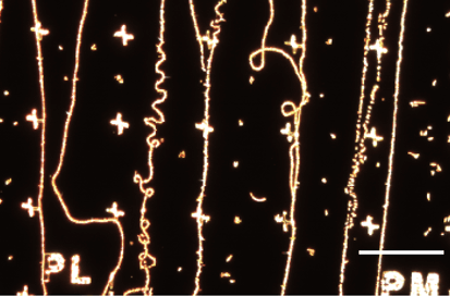
One of the most significant obstacles, if not the most significant, is the difficulty in finding or placing a tube whose diameter is several nanometers (100,000 times smaller than a hair). Together with master's student Gilad Zaevi and doctoral student Michael Schlefman, Prof. Yaish developed a fast, simple, flexible and non-invasive technology for optical imaging of the carbon tubes. The researchers refer to said tubes as a chemical and physical defect on top of the uniform and smooth substrate. This defect serves as a substrate for the crystallization and growth of larger organic nanocrystals, which can be seen and studied with a routine optical microscope (unlike CNTs, which are too small). Since the nanocrystals do not bind to the tubes, they can be vaporized afterward and leave the surface smooth, without damaging the electrical and mechanical properties of the carbon tubes.
"The integrated circuit, the chip, is the biggest breakthrough in electronics so far," explains Prof. Yaish, "and we believe that the method we developed will be a viable platform for integrating nanoelectronics with silicon technologies and perhaps even replacing these technologies with molecular electronics. CNT is an amazing and very strong building block, with wonderful electrical, mechanical and optical properties. Some are conductive and some are semi-conductive, so they are considered a future replacement for silicon. The unique infrastructure in the clean rooms of the Nanoelectronics Center at the Technion headed by Prof. Nir Tesler allows us not only to demonstrate the principle but also to produce world-class devices."
According to Prof. Yaish, the methods that exist today for the production of CNT are characterized by very slow, high cost and inaccuracy in the product - and are generally not applicable to industry. "Our approach is the opposite of the usual. We grow the CNTs in a straight way, and with the help of the organic crystals that coat the tubes, they can be seen under a microscope very quickly. After that, a computer program for image recognition accurately finds the position of the tubes and automatically designs the optimal electrical circuit, and then the device (transistor) can be manufactured. This is the strategy. The target is the integration of nanotubes in an integrated circuit of miniaturized electronic components, mainly transistors on a single chip (VLSI), which may, as mentioned, replace silicon electronics."
Prof. Yuval Yaish studied at Tel Aviv University and graduated with honors with a bachelor's and master's degree in physics. He completed his doctorate - in experimental physics of condensed matter - with Professor Uri Sion at the Technion. He did his post-doctorate in the field of molecular electronics at Cornell University in the USA.
For the full article

8 תגובות
Shimon
You proved to me (again) that religious people are less moral than secular people.
For a secular person, there is no situation that justifies harming another "because emotion has overcome reason".
Religion, in the way you present it, makes me sick.
Shimon In this case my silence is not an admission.
To the honorable Mr. Yossi
The Torah nowhere justifies rape, on the contrary it punishes the rape by providing financial compensation to the family (I suggest you read an article in the book on the subject).
For that matter, there are situations in life where emotion prevails over reason and it is difficult to impossible for an ordinary person to control it. "The Redeemer of Blood" is one doge for that. The wife of Yaft Tavar (which the rabbi is talking about) is another doge.
It is not that the Torah is in favor of rape (the opposite as stated), but rather that where the emotion cannot be controlled, the Torah gave a discount to that person. There is much more to expand on this situation and this is not the place.
The original article
http://www.nature.com/ncomms/2016/160711/ncomms12153/full/ncomms12153.html
The first question can be ignored, I read the article once more and now it is clearer.
Two things are not entirely clear to me:
1. "We grow the CNTs in a straight way, and with the help of the organic crystals that coat the tubes, they can be seen under a microscope very quickly"
I thought the whole thing about nanotechnology is that it's tiny, that each transistor is the size of a few atoms or a few small molecules, here it sounds like it's about something much bigger and massive that can already be seen through an optical microscope... how does that work out? Where is the thumbnail here?
2. "After that, a computer program for image recognition accurately finds the position of the tubes and automatically plans the optimal electrical circuit, and then the device (transistor) can be manufactured."
Interestingly, usually first an optimal electrical circuit is designed, then the circuit components are arranged according to the design. Here it seems that the order is reversed, first the fibers are grown from carbon nanotubes, and only after that the circuit is planned according to the tubes created, it sounds like a somewhat cumbersome and inefficient process, as if first the water tubes are grown, and only then the house is planned and built around them so that it is will fit the shape of the pipes.
The article is called "Automated circuit fabrication" so the professor went to the trouble of allowing the application of a chip. even more beautiful.
To dispel doubt - I never saw it again. This is a main parameter. The equation of motion of the transistor (2) in the article includes a non-linear element - nice. Different from normal transistors. It gives me pleasure to see that the Torah will come out of Zion. Today I opened a newspaper and saw the election of the chief military rabbi and it left a bad taste in my mouth. These are dark forces in the itzela of sheep on the grounds of interpreting the Torah as it is written in 4000 year old texts, without understanding that a part of humanity is trying to refine, to understand and in this part our hopes. I am a traditionalist and articles like this make me cringe. I also read people who are trying to convince Avi Blizovsky that there is no evolution in bacteria for antibiotics, but rather a gene exchange that is characteristic only of bacteria.
The article here changed the taste a little to sweet.
Beautiful - the article. The article is open and you don't have to buy it, which would have zeroed out the number of readers who would have read it through the science. The technology seems very practical. New results for condensed matter are not necessarily used but for experimental measurements and extraction of experimental parameters. It is both practical and beautiful. If the result is a chip that also includes graphene nanotubes, even more beautiful.
I didn't bother to check the power dissipated in the circuit, the ability to place many circuits next to each other, and the speed of the circuits.
Regarding speed, it is probably accelerated (working frequency) because the thickness of the channel in the FET is shortened. Regarding the other two factors - I did not bother to check as mentioned, and they are important factors.
Even in the past, silicon germanium transistors were embedded in a silicon chip in the part that requires the most speed of the external data channel (front side bus). The professor suggests a cautious approach to a chip company, first to a part of the chip and then to the whole chip.