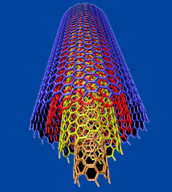
So far, scientists have not been able to produce nanotubes at the high level of uniformity required for electronic systems

Dr. Wei Zhao, a professor in the Department of Chemistry in the Faculty of Mathematics and Science at the University of Arkansas and his student, Xiaomin Tu, currently a post-doctoral fellow at the DuPont Research and Development Center in Wilmington, co-authored an article published in the scientific journal "Journal of the American Chemical Society" regarding The possibility of obtaining the production of nanotubes that are almost perfectly uniform in their dimensions.
The lead researcher said that single-walled carbon nanotubes that are semi-conducting (single-walled carbon nanotubes, SWNTs) and have a diameter of about one nanometer are attracting the most attention as the basis for a new generation of materials as a possible replacement of the silicon in the fields of nanoelectronics . Scientists have not yet been able to produce the nanotubes at the high levels of uniformity that electronic systems require. The research team in question found the way for this. "Our current work combines the selective growth of a few nanotubes and their chromatographic separation in order to obtain an almost complete degree of uniformity in the desired product - a very important step for future electronic applications," says Professor Zahao.
"The semiconductor industry has improved the performance of electronic systems over the past four decades by miniaturizing devices to nanometer sizes. However, this approach will soon encounter both scientific and technological limits." As a possible alternative to this approach, the nanotubes were grown from carbon. However, the lack of structural uniformity of different types of nanotubes with different diameters and chirality is the bottleneck in this field where electronic, photonic and optoelectronic components are used that are required to be uniform in their structure and activity, says the researcher. Dr. Michael Gilt, dean of the Faculty of Science and Mathematics at the university said that the availability of nanotubes with an almost completely uniform structure will greatly speed up the development of new products useful to consumers. "Dr. Zahao's method promises to provide the industry with the necessary raw material for the development of commercial products with increased electronic efficiency, thus helping to conserve energy while obtaining better performance," Gillett said.

One response
Moore's law ticks like a Swiss watch.