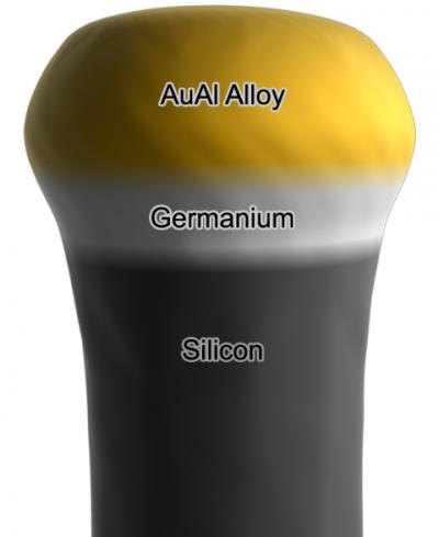
Researchers are now close to using tiny components - semiconductor nanowires to create a new generation of extremely small transistors with defined layers of silicon and germanium, which will enable much better performance of the transistors.

A new generation of extremely tiny transistors from which extremely powerful computer chips can be made using tiny structures called semiconducting nanowires is close to becoming a reality after a joint discovery by researchers at IBM, Purdue University and the University of California, Los Angeles.
The researchers learned how to create nanowires using layers of different materials whose boundary is clearly defined at the atomic level, an essential requirement for making efficient transistors from these structures.
"The success of being able to clearly distinguish between layers of materials allows us to improve and control the flow of electrons and switch this flow as needed - transfer or stop," says Eric Stach, professor of materials engineering at Purdue.
Electronic components are often made of multi-material structures (heterostructures), meaning that they contain well-defined layers of different semiconductors such as silicon and germanium. So far, researchers have been unable to produce nanotubes with defined layers of silicon and germanium. Instead, the transition from one layer to another was so gradual that it could not be optimal for transistor use.
The new inventors point to an approach to creating transistors composed of nanowires.
The findings were published on November 27 in the journal Science. While conventional transistors are built from flat horizontal layers of silicon, the nanoscale silicon wires grow vertically. Because of the vertical structure, they have a smaller footprint, which can make them better suited for transistors on integrated cards or chips, Stach says.
But first one must learn how to produce the nanowires according to strong standards before the industry can start using them to produce transistors," he said.
Nanowires could allow engineers to solve problems that threaten the electronics industries. New technologies will be required for the industry to continue Moore's Law, an unofficial rule according to which the number of transistors in a computer chip doubles every 18 months, which is reflected in the rapid development of computers and communications. Doubling the number of components that can be installed on a computer chip translates to a corresponding increase in performance. However, it is becoming more and more difficult to continue shrinking the electronic components composed of silicon-based semiconductors.

5 תגובות
The main problem today is not the miniaturization but the production of the heat. The formula for heat dissipation of an electronic component
It is E=cVf^2/2 (where E energy, C capacitance, V component voltage, F frequency). When the frequency increases (speed) the heat increases squarely. Therefore, in the last decade, the process scientists at Intel (AMD) have been engaged in parallel calculation and not in increasing the frequency, which is possible with miniaturization, since the electron travels a shorter path. At high frequency the component will burn. It can be minimized for the purpose of parallel calculation, but not for increasing the frequency. There is an alternative technology with reasonable heat called hetero structures. In this method, layers of different materials are produced so that the electron "falls" into a layer with a low energy level, which is not contaminated at all with ions, atoms.
The pollution happens in layers with high energy, so the electron falls to the low energy layer. You can imagine it as a sandwich with 2 slices of bread and chocolate.
However, the distance it travels between collisions is infinitely large (even though quantum convection can be approximated as classical quasi). In GaAs materials, frequencies of 150GHZ can be achieved already with a thickness of 100 microns (and below). The problem is that they are expensive. Materials such as silicon-germanium are used in bipolar components of The data/address channel of computers to speed up the frequency there. Organic materials unlike computers solve the problem in my opinion by parallel calculation in the brain, so we don't burn.
What, don't you see? In this picture there is ice cream flavored with lemon and vanilla!
In such transistors there is no pollution at all. They work in a different way. Additionally, the article doesn't really explain what the other way is clearly.
In any case, it would be nice to get an explanation of what graphene is, what nanowires are, or 0-dimensional systems, SIS, etc.
Such an explanation can help interested readers understand articles of this type. Of course, the great work required is clear.
It is not at all clear how the principle according to which a transistor works is realized here... It is true that the main problem today in the miniaturization process is that the shrinking of the base actually causes an increase in the leakage current and thus a waste of energy and heat emission, but here it is not at all clear what is supposed to be used as Source, Gate, Drain or Base?
Until now, gold has been used as pollution, but using such an amount of gold does not seem to me to make the business profitable at all...
Can I get a link to more information?