This technology may be used in the production of nanometer-sized components, using the way the researchers controlled the concentration of molecules in each pixel.

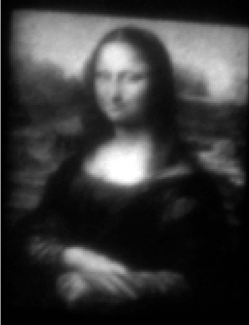
The world famous painting now also comes in a nanotechnology version. Researchers at the Georgia Institute of Technology "painted" the Mona Lisa over an area 30 microns wide, or about one-third the width of her hair. This technology may be used in the production of nanometer-sized components, using the way the researchers controlled the concentration of molecules in each pixel.
The image was created using an atomic force microscope in a process known as ThermoChemical NanoLithography (TCNL) pixel by pixel (125 nanometers in diameter). The researchers placed a heated support on a substrate and created a series of chemical reactions on a nanometer scale. By changing the level of heating at each point, the researchers controlled the number of new molecules formed. The higher the heat, the greater the local concentration of molecules. More light created the lighter shades of gray in Mona Lisa's forehead and hand. Heating to a lower temperature created the dark shadows in her dress and hair.
"By controlling the temperature, our team manipulated the chemical reactions to provide variations in the concentration of molecules on the nanometer scale," says Jennifer Curtis, assistant professor in the School of Physics at the Georgia Institute of Technology and principal investigator. The spatial confinement of each such chemical action in a limited space was required to create a complex image like the Mini Lisa".
"We predict that the TCNL will be able to perform such subtle operations also for example in controlling the conductivity of graphene" says Curtis. "This technique could enable a wide variety of experiments and applications that were previously impossible in fields such as nanoelectronics, optoelectronics and bioengineering.

3 תגובות
You're right, I should have put the word 'cloth' in quotes.
It is likely that the fabric was not used (as opposed to what is written in the title)
You should fix the title.