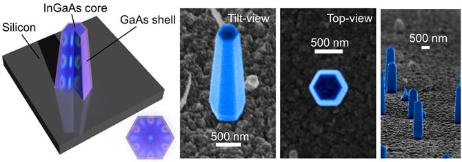
Engineers at the University of California, Berkeley, have found a way to attach nanolasers directly to a silicon surface, an achievement that could lead to the development of a new family of faster and more efficient microprocessors, as well as powerful biochemical sensors using optoelectronic chips.

The research findings were published in the scientific journal Nature Photonics.
"Our research findings have implications for a wide range of scientific fields, including materials science, transistor technology, laser science, optoelectronics and optical physics," said principal investigator Connie Chang-Hasnain, professor of electronic engineering and computer science.
The ever-increasing performance requirements in electronics have led many researchers to search for better ways to harness the inherent ability of light particles to transmit much more information than electrical signals can. Optical connections are considered as a solution that can overcome the bottleneck in communication within and between computer chips.
Since silicon, the material at the base of today's electronic components, is an extremely poor producer of light, engineers have turned to another family of materials known as III-V (family three-five) semiconductors to create light-based components such as light-emitting diodes (LEDs) and lasers .
However, the researchers discovered that the fusion of these materials and silicon to produce a combined optoelectronic chip was problematic. First, because the atomic structures of the two substances are incompatible.
"Making layers of 3-5 semiconductors on silicon is like forcing two incompatible pieces of solder together," said lead author Roger Chen of the University of Berkeley. "This is possible, but the materials are damaged during the process."
In addition, the manufacturing industry is adapted to the production of silicon-based materials, and therefore, due to practical reasons, the goal until now has been to integrate devices based on semiconductors from this family within existing infrastructures, the researchers explain.
"The infrastructure of silicon-based electronic components is so large today that it is difficult to change, both for economic reasons and for technological reasons, so the level of compatibility for production with silicon is essential," explains the researcher. "One of the problems is that the creation of semiconductors from this family usually involves processes that use high temperatures - 700 degrees Celsius or more - which will destroy the electronic components. Meanwhile, other integration approaches have not yet been adapted to industrial scale.”
The researchers found a way to overcome this problem by growing nano-pillars composed of indium-gallium-arsenide, a material from the 3-5 family, on a silicon surface at a relatively "cold" temperature of only 400 degrees Celsius.
"Working on a nanometer scale allowed us to grow materials from the 3-5 family of high quality at temperatures low enough to be suitable for silicon-based electronic components while preserving their original activity," said the researcher.
The researchers used a metal-organic CVD (chemical vapor deposition) method to grow nano-pillars using silicon. "This method could enable industrial production capacity, because this system is already used commercially to create solar cells containing tiny layers and light-emitting diodes," said the researcher.
From the moment the nano-pillar was obtained, the researchers showed that it is capable of emitting laser light in the near-infrared range - a wavelength of about 950 nanometers - at room temperature. The hexagonal configuration, dictated by the crystal structure of the nano-pillars, produces an innovative and efficient light-trapping optical niche. The light moves freely up and down through the structure in a spiral manner and is amplified through this optical feedback mechanism.
The unique approach of growing nanolasers directly on silicon surfaces could lead to very efficient silicon-based photonic components, the researchers note. The researchers explain that the small dimensions of the nanopillars allow them to be stacked one on top of the other into small piles with low energy investment.
"Ultimately, this method could provide an innovative and efficient route to create nanophotonic devices on a chip such as lasers, photo-sensors, modulators and solar cells," say the researchers.
"This is the first time that a bottom-up method has been applied to connect type 3-5 nanolasers to silicon chips through a growth process that is compatible with the technology currently used to create metal oxide semiconductors and printed circuits," explains the researcher. "In our research lies the ability to accelerate an opto-electronic revolution in the fields of computers, communications, monitors and optical signal processing devices. In the future, so the researchers hope, it will be possible to further improve the characteristics of these lasers and eventually achieve control over them in order to combine electronic devices with photonic devices."

4 תגובות
Hahaha... without graphene, rather a refreshing change
Are there any relevant nanotoxicology studies (I don't know if that's how they prescribe)
Many nano materials are created today, what are the environmental effects of all of these?
And all this without involving even one graphene atom. disappointing
Please buy the link to the original news.
In addition, opening blockages in the blood vessels in the heart or other parts of the body, legs, genitals, etc.