A new technology developed by a researcher at the Technion, during her postdoctoral research at the University of Chicago, is expected to bring about a dramatic breakthrough in the miniaturization of electronic devices. The study, in which researchers from the University of Chicago and Argon Laboratories in Illinois participated, was led by Dr. Tamar Segal-Peretz, currently a member of the faculty at the Wolfson Faculty of Chemical Engineering at the Technion
A new technology developed by a researcher at the Technion, during her postdoctoral research at the University of Chicago, is expected to bring about a dramatic breakthrough in the miniaturization of electronic devices. The study, in which researchers from the University of Chicago and Argon Laboratories in Illinois participated, was led by Dr. Tamar Segal-Peretz, currently a member of the faculty at the Wolfson Faculty of Chemical Engineering at the Technion.
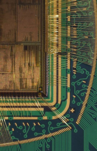
The research, published in the journal ACS Nano, focuses on the self-assembly of block copolymers - polymer chains used as templates in manufacturing processes (nanofabrication). The article presents a new approach to the production of nanopatterns in the self-assembly processes of block copolymers. This approach enables production in dimensions smaller than 10 nanometers, which are considered a complex challenge in the microelectronics industry.

To the depth of the layers
Miniaturization to small dimensions and the use of block copolymers require an in-depth understanding of the processes that take place in the depth of the layers, and according to Dr. Segal-Peretz, "most of the tools that exist today only examine the surface of the material, thus missing important information that lies beneath the surface."
The research now being published shows that the new approach - three-dimensional mapping of the structures using tomography in penetrating electron microscopy (STEM tomography) - is essential for understanding self-organization processes and for creating nanopatterns of a much higher quality. "Combining molecular simulations with the XNUMXD information collected allows us to understand the interactions between the copolymers and the templates on the substrate and the origin of the spatial fluctuations in the nanostructures."
The researchers estimate that in this research they are paving the way for the design and production of improved templates for the creation of electronic components whose size does not exceed 5 nanometers - much smaller than the current components produced by photolithography, i.e. by projecting light through a mask. In photolithography, the wavelength limits the miniaturization of patterns for production. For small devices, short wavelengths are needed, and producing such stable radiation is a more difficult task. According to Dr. Segal-Peretz, "the advantage of block copolymers is that the size of the template is determined by the chemistry of the polymer and not by an external factor such as wavelength."
Directed self-organization
However, self-organization alone is not sufficient for production purposes, because the position of the patterns created in this way is not controlled. "In order to direct the polymers to the desired position, we make an initial template, which is very easy to make, and it directs the polymers. This process is called directed self-assembly. Combining this approach with existing photolithography processes allows us to overcome the limitations in nanopattern production, while maintaining a low cost."
As mentioned, one of the challenges in the production of electronic components is the existence of defects in the pattern. This is a scientific and technological problem because without a full identification of the defects below the surface, it is impossible to understand the source of the defects and therefore it is impossible to develop improved production methods. "Ultimately, the world is three-dimensional," says Dr. Segal-Peretz, "and therefore no two-dimensional representation of it is satisfactory."
Three degrees at the Technion
Dr. Tamar Segal-Peretz completed her entire degree at the Technion - after a bachelor's degree in biochemical engineering at the Faculty of Chemical Engineering, she worked in industry developing night vision systems, and then went on to a direct doctorate within the Russell Berry Nanotechnology Institute (RBNI). She did her doctorate under the guidance of Prof. Giti Frey at the Faculty of Materials Engineering on polymer-based solar cells. After a post-doctorate at the University of Chicago and the Argonne National Laboratory, she joined the faculty of the Wolfson Chemical Engineering Faculty.
