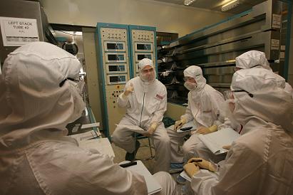
The entire project is designed to create a state-of-the-art framework for educating engineers and researchers in a combination between existing technologies and future occupations. It was funded by the European Union, which chose the Technion to lead it

Twelve young scientists from Europe and Malaysia, all of whom have a doctorate or are in the advanced stages of completing it, went through a practical training course at the Technion, on the subject of the integration between the micro and the nano. Later, five more courses will be held at the Technion, in Rome (Italy), and in Grenoble (France). The entire project is designed to create a state-of-the-art framework for educating engineers and researchers in a combination between existing technologies and future occupations. It was funded by the European Union, which chose the Technion to lead it.
The young scientists worked and studied in the "clean rooms" at the Technion's Microelectronics Center, and at the Zisapel Center for Nanoelectronics. They learned about the interdisciplinary aspects and the transition from "traditional" methods of microfabrication ("clean rooms") to a new environment that will combine innovative materials with the development of cutting edge nano technologies.
Professor Yosef Salzman, director of the Technion's Microelectronics Center, said that the scientists were exposed to the required theoretical background and experienced various aspects of microfabrication and nanofabrication.
"The participants understood the need for the integration of procedures, and took an important step in training them to work in the future nanoelectronics laboratories," he emphasized. "The materials, methods and equipment widely used in nanotechnology are not always suitable for conventional production in clean rooms. It is interesting that despite the understanding that the microelectronics production environments that exist today will not allow the absorption of some of the new technologies, there are no courses in the world that deal with the problem at an in-depth level. Therefore, the framework created here is arguably a breakthrough in the education of future engineers."
At the end of the six courses, a three-day workshop will be held on the fusion of traditional microelectronics with nanotechnology, in Grenoble, France, in the summer of 2009.
