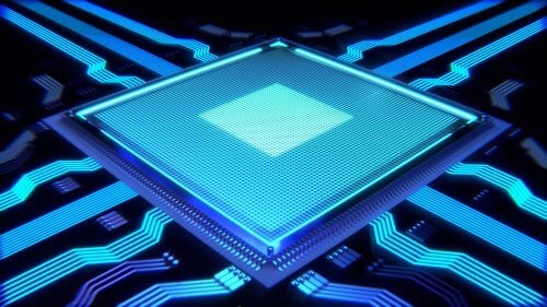
Researchers at IBM presented five papers at the International Society for Optics and Photonics (SPIE) conference focusing on the possibility of continuing to build on extreme ultraviolet technology and extending it to 5 nm and even 3 nm chips. In order to succeed in this miniaturization process, all aspects of the production equipment, materials and production processes must be taken care of - and brought to the limit of possible performance.

At the end of 2017, IBM introduced the new generation of extremely high-performance hardware systems, designed for cognitive computing and artificial intelligence applications: POWER9 chips integrated into the world's most powerful supercomputers, Summit and Sierra. At the same time, IBM also introduced a new z14 model mainframe, which for the first time offers full data encryption capabilities - from end to end - in a way that is particularly suitable for the requirements of the digital economy era.
This progress in the field of hardware is based on 14 nm production technology, which was developed in IBM's research laboratories at the beginning of the current decade. In addition, IBM also reported on its future development pipeline in the field, designed to accelerate computational capacity in the field of artificial intelligence. Thus, alongside the progress in the field of quantum computing - research and development in the field of silicon technologies continues to promote modern computing. IBM is steadily expanding the performance range of silicon-based logic circuits. On the way to the production of chips with a resolution of 7 nm and 5 nm, IBM and a number of companies working in cooperation with it are establishing ultra-violet light lithography at an extremely short wavelength (Extreme Ultraviolet - EUV, extreme ultra-violet). This technology enables a significant minimization of the size of the transistors - which will allow a larger number of components to be compressed into one piece of silicon.
Four years of accumulated experience in operating production systems in ultraviolet lithography, gave birth to a professional article dealing with "characterization and control of an EUV scanner to display uniformity and stability". The article describes the methods by which it is possible to ensure that the ultraviolet light used to burn "production masks" of chips will be projected uniformly and accurately. Although the current exposure control methods are far from perfect, characterization and control technologies can improve performance.
Expanding the use of ultra-short ultra-violet light lithography until the full extraction of the photocatalyst stored in it will require a re-examination of some of the existing assumptions concerning the lithography process itself. In another paper presented at the conference, one of the IBM researchers examines the physical and chemical process of lithography, in order to present new ways with the help of improvements in the chemical solutions used to develop the image. The article opens what is perceived as a "black box", in which the development process is carried out - in a way that presents new possibilities for the use of improved development materials in the production processes of 5 nm chips.
Two other articles examine the use of brushing of polymers as a tool to improve the embedding of circuit patterns when exposed to extremely short ultra-short-wavelength light, as well as new production processes of silicon masks - the combination of which is expected to enable the production of chips even at 3 nanometers.
Masks used in the production processes of computer chips allow light to be irradiated in the patterns and lines required to imprint the intended chip structure on the silicon wafer. The silicone is applied in a thin layer of light-sensitive material - similar to the way traditional photographic film works. The projected light outlines conductive lines and junctions where these lines cross, in order to create a transistor structure at each point of intersection. Extremely short wavelength ultraviolet light (EUV) operates outside the spectrum visible to the human eye, at a wavelength of 13.5 nanometers or less - which is significantly shorter than the wavelength of deep ultraviolet (deep-UV) used in previous generation technologies, which is 193 nanometers. Such a short wavelength requires a high level of precision in the construction of the mask used to create the image. Similar to high-definition television, which allows us to see more details in the image - in EUV lithography, defects in the mask and deviations from the orderly structure will be more significant and will have a greater impact on the final result.
In order to move from experiments to production on a large scale, tools are needed to detect defects in production and processes that will make it possible to understand the factors affecting the output levels of normal chips (yield). Here, IBM researchers present new methods that make it possible to advance the production processes of silicon chips whose conductive band thickness is no greater than that of a few DNA molecules - produced in large quantities, on silicon wafers with a diameter of 12 inches.

2 תגובות
True, because we have already seen the enormous scientific successes of the communist countries in promoting science and sharing scientific and technological knowledge between them and the rest of the world. Recently, even Venezuela manages to show us where the fish urinates from and its progress in all scientific fields.
If only these pigs would share knowledge instead of selling
In all 100 years of their existence the world would look more beautiful but the face of pig capitalism