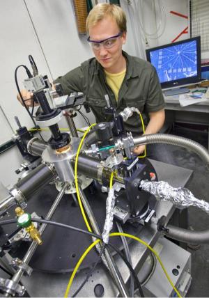
The feature will be important for the construction of solar cells composed of nanocrystals, and for the use of solar energy to produce clean and renewable liquid fuels for transportation,

In a development that holds great promise for the future of solar cells composed of nanocrystals, and for the use of solar energy to produce clean and renewable liquid fuels for transportation, researchers from the US Department of Energy reported a novel method by which the electrical conductivity of nanocylindrical crystals of the semiconductor cadmium- Selenide a hundred thousand times.
"The key to our success is the production of electrical contacts made of gold at the ends of the cadmium-selenide cylinders by their direct growth from a solution layer," explains the research center, Paul Alivisatos. "Solution-derived contacts provide a tight metal-nanocrystal interface without surfactants or other additives, and unlike previous methods for making such contacts, our state-of-the-art method preserves the inherent semiconducting nature of the original nanocrystal."
In light of the forecast, that the global demand for energy will double by 2050 and even triple by the end of the twenty-first century, there is an immediate necessity for the development of stable and carbon-free energy technologies. The use of solar radiation to generate electricity as well as to split water for the preparation of fuels is considered a vision of the best energy source, and nanocrystals may be an essential part in advancing this vision. Electrical conductivity in semiconductor nanocrystals is an essential characteristic for both solar energy and fuel cell technologies.
"Normal processes for making contacts, in which metal is directly adsorbed to the semiconductor nanocrystals, and which are used today in the production of commercial chip layers, cause structural defects and unwanted chemical reactions at the interface between the metal and the semiconductor," the researcher notes. "In other words - the finished electrical device actually consists of a different material than the original nanocrystal."
The researcher points out that while chemical methods, such as the addition of surfactants, resulted in an increase in electrical conductivity in tiny layers composed of solid nanocrystals, these methods often result in changes in the electrical properties of the semiconductor, for example - changing the material from n-type to p-type, or changes in its density. Moreover, previous studies were unable to explain why the electrical conductivity increased, other than referring to the fact that the surfactant coating was removed.
In this study, the team of scientists used electrical measurements of a single nanostructure to make a systematic comparison between cadmium selenide nanocylinders with gold edges and those without them. The process of creating the edges began with the addition of a gold salt to a solution of toluene and cadmium-selenide nano-cylinders, which caused the selective adsorption of the gold metal to the ends of the nano-cylinders. In the next step, a layer of silicon (the essential component of the chip) was immersed in this solution. After evaporating the solvent of the solution (toluene), individual cadmium-selenide nanocylinders were obtained arranged along gold electrodes prepared in advance using electron beam lithography. The end result was uniform-structure cadmium-selenide devices with gold contacts placed on their ends.
"Our study shows that the improved performance of uniform gold-tipped cadmium-selenide structures originates from a lower Schottky barrier and that solution-derived contacts do not change the chemical composition of the semiconductor. In addition, our research demonstrates the increasing sophistication of high-quality electronic devices that can be obtained through self-assembly processes, and the ability of these processes to be an excellent way to develop the next generation of electronic and opto-electronic devices using nanocrystals."
"We believe that our approach is the best method for preparing future devices from nanocrystals since it preserves their original semiconducting nature along with precise synthetic control of their production," notes the lead researcher.
According to the researchers, the next step in their research will be to determine if the sharp improvement in the electrical behavior can be translated into an improvement in the energy production itself. Initially, the group of scientists intends to investigate the use of solution-derived contacts in photovoltaic applications.

One response
Can you please explain some of the articles on the site in simpler language. Because there are readers (I am among them) who find it difficult to understand articles like this one because of the scientific terms that are not that familiar to them.
Thanks.