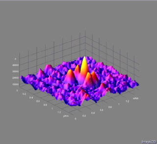
The new method, known as nanocrystallometry, makes it possible to create precise components for use in the field of nanotechnology

Researchers have announced the first-ever method to control the growth of metal crystals from individual atoms. The new method, known as nanocrystallometry, makes it possible to create precise components for use in the field of nanotechnology.
The findings of the study, conducted at the University of Warwick, have long been published in the scientific journal Nature Communications. Professor Peter Sadler from the chemistry department at the university points out that: "The breakthrough in our nanocrystallometry method lies in the fact that it allows us to actually directly observe and control the nanoscale world in motion."
By using a graphene substrate into which a foreign substance was introduced, and which was designed to slow down their movement and eventually trap the atoms of the precious metal osmium, the researchers were able to control and quantify the growth of metal crystals. When the trapped atoms come into contact with additional osmium atoms they bond together, eventually growing into three-dimensional metal crystals.
"Determining the exact structures of nanoscale objects is of great importance for the production of the materials of the future," explains one of the researchers. "Until now, the production of metal nanocrystals, which are essential for these future materials, has not allowed high-precision control of individual atoms, under mild conditions."
Says the lead researcher: "The importance of our innovative method lies in the fact that it enables the preparation of nanometer metal crystals with a size of only 15 angstroms. If a nanodevice requires a million osmium atoms, then from one gram of this material we can produce about 400 thousand devices. Compared to existing methods, our method provides a considerable improvement in the economic aspect and in terms of the production efficiency of nanometric objects with precise structures."
The researchers note that their method could be used in a variety of applications. "We believe that with the help of our method it will be possible to build precise electronic circuits at the atomic level as well as nanodevices for storing information. The method also has significant potential in the fields of bio-sensing of drugs, DNA and gases, as well as in the creation of unique nanopatterns on surfaces for security labeling and sealing of confidential documents. The method could also be used in the production of new metal nanoalloys, and combinations of other interesting materials. It is possible that these future materials will have particularly unusual properties that have not yet been discovered," says one of the researchers.
The new method is based on the use of a sophisticated and advanced TEM microscope (penetrating electron microscope, Wikipedia) which is only at the University of Warwick in the UK, and which allows the observation of individual atoms. We all know that the whole world is made up of atoms, but it is really rare to see them moving in front of your wondering eyes," says one of the researchers.

One response
Missing link to the article...