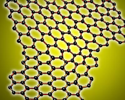
The material Graphene, a single layer of carbon atoms connected to each other in a pattern of hexagons, like a beehive structure, has the ability to be used in nanoelectronics such as: memory, opto-electronic devices and the like.

The preparation of an extensive graphene surface on copper may enable the production of state-of-the-art graphene-based devices that meet the standards requirements of the semiconductor industry and lead to the development of faster computers and electronic components - according to a team of scientists and engineers from the University of Texas.
"The material graphene could lead to the development of faster computers that use less energy, and to other types of communication devices such as high frequency devices (radio frequency waves)," said physical chemistry professor Rod Ruoff, one of the authors of the article in the scientific journal Science. "It will also be possible to find use for it in electrically conductive and optically transparent layers for image display technology and in the use of generating electric power from solar cells."
The material Graphene, a single layer of carbon atoms connected to each other in a pattern of hexagons, like a beehive structure, has the ability to be used in nanoelectronics such as: memory, opto-electronic devices and the like. It could also be used for electrical energy storage in batteries and capacitors, in the field of composite materials, thermal treatment, biochemical sensors and as a new sensing material for highly sensitive pressure sensors.
"Today there is an essential requirement for the preparation of graphene coatings on silicon layers using methods adapted to the processes that exist in the semiconductor industry," said the researcher. "This way it will be possible to prepare nanoelectronic circuits with extraordinary efficiency, an efficiency that is so important to the semiconductor industry."
Graphene exhibits extremely high mobility of electrons and their holes; As a result, the switching speed of graphene-based nanoelectronic devices can be extremely high. Also, the graphene exists in a flat form when it is placed on a substrate such as a Zorn layer and therefore it is adapted to the processes of processing the layers in the semiconductor industry. The unusual mechanical properties of graphene could enable its use as a membrane material in nano-electromechanical systems such as a highly sensitive pressure sensor and as a detector of chemical separations or biological cells.
The team of researchers was able to place graphene on copper foils whose area is limited only by the type of machine used. They demonstrated, for the first time, that areas with a size of one square centimeter can be coated, almost completely, with a single layer of graphene, when only a very small percentage (less than five percent) of the area is obtained as a bi- and tri-layer. In the next step, the team prepared double-gate transistors where the upper gate is electrically isolated from the graphene layer by a tiny layer of alumina (ceramic oxide) in order to measure the mobility of the charge carriers. The devices showed that mobility, a main characteristic of electronic devices, was significantly higher than that existing in its form - the main semiconductor used in most electronic devices today, and comparable to natural graphite.
"We used a method of chemical vapor deposition (CVD - chemical-vapor deposition) from a mixture of methane and hydrogen to place a graphene layer over copper foils," explains the researcher. "The low solubility of carbon in copper, and the ability to achieve a high grain size in the polycrystalline copper substrate are attractive factors for its use as a state-of-the-art material in nanoelectronics - and in addition there is the fact that the semiconductor industry has comprehensive and extensive experience in the use of tiny copper surfaces coated with zinc layers. Through the use of diverse characterization methods, we were able to conclude that graphene-coated copper is a very promising material for the future development of 300-millimeter pieces of iron coated with high-quality graphene."

One response
Stunning!
And graphene was only discovered in 2004.
And it is so basic and simple as if waiting to be revealed.