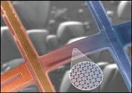
Researchers from the Federal Research Laboratory in Switzerland prepared graphene-like materials using a chemical route that utilizes metal surfaces

Graphene is a promising material for the development of nanoelectronic devices in the future. However, the search for precise and industrial methods to prepare graphene, and materials derived from it that have electronic properties, is still in progress. In order to overcome this limitation, researchers from the Federal Research Laboratory in Switzerland prepared graphene-like materials using a chemical route that utilizes metal surfaces.
The work has just been published in the scientific journal Nature Chemistry. In this study, the scientists combined empirical observations derived from scanning tunneling microscopy (STM) together with computer simulations.
Electronic components are becoming increasingly tiny, with microelectronic components being gradually replaced today by their nanoelectronic counterparts. In the nanometer world, silicon (silicon), which is today the most common material in the field of semiconductors, is beginning to reach the limits of its use, which prevents further miniaturization and technological progress. Therefore, the demand for new materials to be used in the field of electronics is great. Thanks to the excellent electronic properties of graphene, which is a two-dimensional network of carbon, it is considered a possible alternative. However, several hurdles must be overcome before graphene can be used in the field of semiconductors. For example, today there is no easily applicable method for preparing graphene-like materials on a large scale.
Researchers from the Swiss Federal Research Laboratory (Empa, nanotech@surfaces) have reported the development of a surface-based chemical route to prepare small sections of graphene, forms known as nanographenes. By using a model of a starting material of the polyethylene type, the researchers were able to discover, together with their partners from a German institute (Max Planck Institute for Polymer Research in Mainz), and from the University of Zurich, how the reaction takes place in detail on a copper surface and how the building blocks can be converted into nano - Planar graphenes directly by the surface.
To obtain their findings, the researchers combined empirical observations, particularly from a scanning tunneling microscope, along with computer simulations. The simulations were used to determine in advance whether a chemical reaction is theoretically possible, or not, in light of the considerations of the energy involved. The results: the reaction pathway consists of six steps and five intermediates. Two of these intermediates are stabilized with the help of the surface, so that they can be seen as an image using the particular microscope. The energetic barriers between the various intermediates are reduced thanks to the catalytic effect of the substrate.
However, in order to be able to integrate them into electrical circuits, the graphene-like materials must be produced using semiconductor surfaces instead of metal surfaces. The researchers examined their simulations to check if their approach could also work on these surfaces and the findings are very promising and show that substrate-based synthesis is a possible way to produce nanographenes on demand on a variety of surfaces and substrates.

2 תגובות
Already today I see pieces on the beach that are made of graphene
What are the chances that we'll see chicks on the beach wearing kini made of graphene?