The connection of sheets of material with a thickness of one atom creates materials with completely new properties and opens a window to amazing possibilities * Human progress has always been closely related to the discovery of new materials and Lego blocks on a nanometer scale are something that has never been seen before.
Generations of smart minds have been inspired by Lego: the small plastic blocks that connect to each other. These cubes became imaginary cars, sprawling castles and other creations greater than the sum of their parts. Today, an entire generation of materials scientists is being inspired by a new kind of Lego: atomic-scale building blocks.
These new building blocks are thin sheets of material that can be as thick as one atom and that can be stacked on top of each other in an orderly and precise manner. This unprecedented precision in building materials can enable the production of materials with optical and electrical properties that were previously impossible to achieve. These features allow scientists to imagine future applications such as devices that will consist of materials whose electrical resistance is almost zero, computers that are faster and have greater computing power than computers available today, and electronic gadgets that are light enough to be worn, bent and folded.
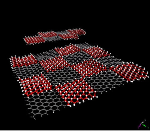
This breakthrough resulted from the creation of a material called graphene, which consists of a single sheet of carbon atoms. My colleagues and I at the University of Manchester in England isolated this material from a thicker block of graphite in 2004. We created the graphene sheet, a material that at the atomic level consists of a two-dimensional surface of hexagons, and therefore looks a bit like chicken coop fencing netting, by peeling off one-atom-thick layers from the end of a block of graphite using adhesive tape. Over the past ten years, researchers have managed to find several dozen more crystals from which two-dimensional sheets of material can be pulled out in a similar way, and the number of these crystals continues to increase rapidly. Mica (mica) is one example of such a crystal and so are materials with exotic names such as hexagonal boron and molybdenum disulphide.
These sheets of crystals are considered two-dimensional because the thickness of a single atom is the minimum thickness that any material can reach. (It is also possible to use slightly thicker crystals, say three atoms thick.) The other dimensions of these two-dimensional sheets, namely their length and width, can be much larger, depending on the goals of the material creator. In recent years, two-dimensional crystals have become a hot topic in materials science and solid state physics because they have many unique properties.
These layers can be stacked in fairly stable ways, even though they don't bond together in the usual chemical way, for example covalent bonds where atoms share electrons with each other. Conversely, in these materials, atoms from adjacent layers are attracted to each other by weak forces known as van der Waals forces. Normally van der Waals forces are not strong enough to hold atoms and molecules together, but because the two-dimensional crystal sheets are so large and packed with atoms and so close together, these forces add up and become very strong.
To understand the tantalizing possibilities of engineering such materials, consider, for example, superconductivity at room temperature. For generations scientists have been trying to transmit electricity without energy losses and to do so without having to cool the electrical devices to extremely low temperatures. If materials are found that make this possible, the consequences for our civilization will be far-reaching. There is a broad consensus that, in principle, this goal is achievable, but no one knows how to achieve it. The highest temperature at which materials become superconducting is below minus 100 degrees Celsius, and in the last twenty years there has been little progress in raising this limit.
We recently learned that there are some superconductors made of oxides, meaning compounds of elements with oxygen, that can be split into two-dimensional layers in the way I described above. And what will happen if we reassemble these layers, in a different order, and insert other crystalline layers between them? We know that superconductivity in oxides depends on the spacing between the layers and that adding more layers between the crystal planes can turn some materials that are poor conductors, or even insulators, into superconductors.
This idea has not yet been fully tested, mainly because the technology of creating Lego on an atomic scale is still in its infancy. Undoubtedly, it is difficult to assemble complicated multi-layered structures. Nowadays, it is rare for such structures to contain more than five different layers and they are usually built from only two or three types of Lego blocks. It is usually graphene combined with two-dimensional crystals of nitrogen boron, which is used as an insulator, and of superconductors such as molybdenum disulfide and tungsten disulfide. Because these layered stacks contain several materials, they are often referred to as "heterostructures". Currently these heterostructures are quite small, typically no more than about 10 microns in length and width, less than the cross-sectional area of a human hair.
With these layered stacks we can conduct experiments in search of new electrical and optical properties as well as new applications. For example, a fascinating aspect of these layers is that despite their thinness, they are quite flexible and transparent. These features may enable the development of light-emitting devices that can be designed in different ways, for example display screens that can be folded and unfolded according to the user's needs. Another option is computer chips with high energy efficiency.
If these experiments yield an important discovery, we believe that it will be possible to transfer the technology to an industrial scale. This has already happened with graphene and other two-dimensional crystals: initially they were produced as crystals a few microns in size, but now it is possible to produce them in sheets with an area of up to hundreds of square meters.
Although no groundbreaking application of these materials has yet been reported, advances in the field are creating a buzz of excitement in scientific communities. Human progress has always been closely related to the discovery of new materials. Such discoveries were the cause of the transitions between the stone, bronze, iron and silicon ages. Lego bricks on a nanometer scale are something that has never been seen before and right now there seems to be no limit to what they will allow.
About the author
Andre K. Geim is a physicist at the University of Manchester in England. In 2010 he won (jointly) the Nobel Prize in Physics for his work on graphene.
The article was published with the permission of Scientific American Israel
Carbon Wonderland - About the 2010 Nobel Prize Winners in Physics, Scientific American
Graphene - the most perfect atomic lattice of all
New from Andre Game - Teflon made of graphene
