The researchers succeeded in replacing the individual carbon atoms in graphene with boron and nitrogen atoms, while obtaining a two-dimensional hexagon-like network with the properties of a semiconductor, i.e. - a version of graphene capable of performing electrical switching operations

[Translation by Dr. Nachmani Moshe]
Single-atom-thick semiconductors are no longer the stuff of science fiction. A new two-dimensional material could bring about a revolution in the field of electronics, according to the researchers.
Professor Axel Enders from the University of Bayreuth (Bayreuth) in Germany, together with his research colleagues from Poland and the USA, developed a two-dimensional material that could revolutionize the field of electronics. Thanks to its semiconducting properties, this material could be more effective in the fields of high technology than the material graphene, for which the Nobel Prize in Chemistry was awarded. The new material includes carbon, boron and nitrogen and its chemical name is: "hexagonal boron-carbon-nitrogen" (h-BCN). The research has long been published in the scientific journal ACS Nano.
"Our findings could be the main point of a new generation of transistors, circuits and electronic detectors that will be much smaller than electronic components that exist today and, in addition, can be bent. Moreover, electronic components that will be based on the new material will be able to significantly reduce their electricity consumption," said the lead researcher. Still, the technology has limitations associated with further miniaturization. "Our new material is much more suitable than graphene when it comes to pushing the boundaries forward," claims the lead researcher.
The material graphene is a two-dimensional lattice composed entirely of carbon atoms. That is - its thickness is a single atom failure. As researchers progressed in the study of this material and its structure more and more, they discovered its extraordinary electronic properties that were received with enthusiasm throughout the entire scientific world. Graphene is 300-100 times stronger than steel, and at the same time it is also an excellent conductor of electricity and heat. At the same time, the electrons can move without limit at any electrical voltage and thus there is no off/on state. "Due to this reason, the material graphene is not particularly suitable for most electronic devices. In such a situation, semiconductors are needed, since only these can guarantee switching capabilities (on/off state)," explains the chief researcher.
The researchers succeeded in replacing the individual carbon atoms in graphene with boron and nitrogen atoms, while obtaining a two-dimensional hexagon-like network with the properties of a semiconductor, i.e. - a version of graphene capable of performing electrical switching operations.
Article Summary
The news about the article
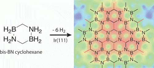
The chemical reaction to create two-dimensional graphene that includes boron and nitrogen atoms, in addition to the original carbon atoms.

One response
Many points are unclear from the article and there is no reference to the source.
What is the direction of the current? What is the switching factor?