A smart device, based on a single atomic layer, which sorts and controls the spin of photons, may lead to the development of next-generation computers
Individual atomic layers of materials (or 100D materials) have unique optical and electronic properties that do not exist in normal scale materials. When we think of the properties of matter, we usually assume that they are based solely on the constituents of the matter. For example, a metal conducts electricity because its atoms are held together by metallic bonds, which leave free electrons that can move through the material when an electric field is applied to it. However, there are other factors that can affect the behavior of a material: for example, its size. This is especially true when the dimensions of the material are reduced to XNUMX nanometers or less (a nanometer is one millionth of a millimeter). Electrical conductivity, chemical reactions, mechanical properties and even the way a material interacts with light - all these can change in a material whose size is reduced to the level of a few nanometers. As our ability to create and study materials in the nanometer range has progressed, new, fascinating and unexpected properties are revealed, which opens completely new avenues for future technologies that rely on the size of the material as well as its basic properties.
What is the question? How can the spin property of the light particles be controlled?
Nanoscale materials can be classified according to the total number of their nanoscopic dimensions. For example, if all three dimensions of the material are of nanometer size, the material is called zero-dimensional, or by its better known name: nanoparticle. If two dimensions of a material are nanometer in size, while the third dimension is much larger (similar to a piece of string shrunk to a tiny size), scientists say it is a one-dimensional material ("tube", or "nanowire"). If only one dimension is nanometer-sized, the material is two-dimensional, similar to a large but very thin sheet (like a piece of paper).

Another class of materials are metamaterials: artificial nanoscale structures that do not exist in nature. A unique category of these engineered materials is the group of meta-surfaces: thin two-dimensional artificial structures produced with innovative technologies that maintain unique interactions with light through small optical nanometer "antennas", which enable the design of wave fronts. Prof. Hasman's research group, at the Technion, laid the foundations for the field of optical metasurfaces, which is currently considered one of the hottest fields in optics. The technology developed by Prof. Hasman's laboratory - among other things with the help of a research grant from the National Science Foundation - makes it possible to realize very precise insulating metasurfaces made of silicon, without metals, that do not absorb light.
After the discovery of graphene, a two-dimensional semiconductor material made of a single layer of carbon, and the study of its unique properties, many other two-dimensional semiconductors were discovered and developed. In these materials there may exist an essential condition called "direct energy gap" which does not exist in silicon. The lack of an essential state in silicon is a technological limitation in the integration of electronics and photonics, which is considered a combination that may help the development of the next generation of computers. The discovery of a direct energy gap in XNUMXD materials now makes it possible to combine nanoscale photonics and electronics to create future computing components.
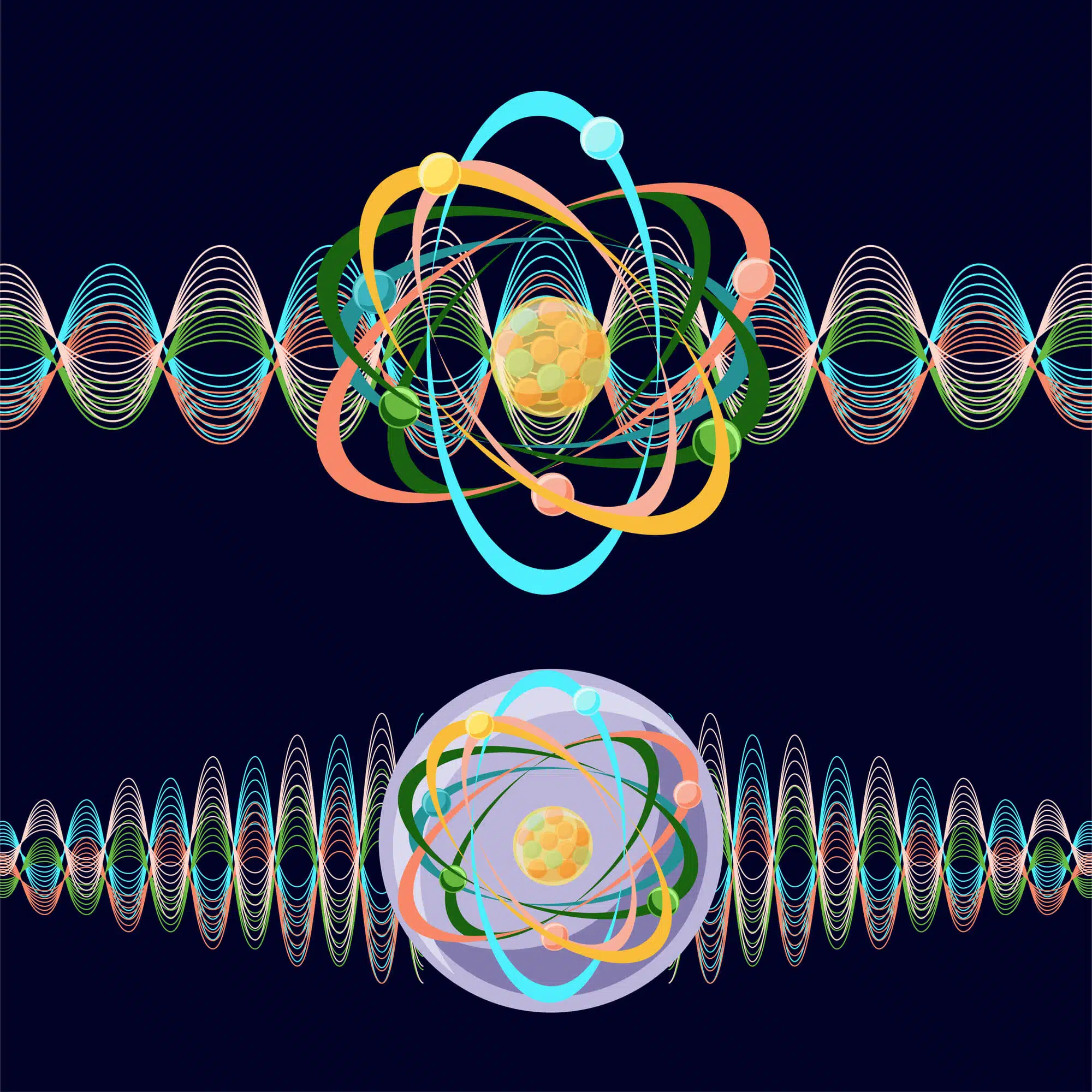
The members of Prof. Hasman's research group, in collaboration with the research group of Prof. Elad Koren, also from the Technion, developed a device based on a single atomic layer of tungsten selenide, capable of manipulating light (photons) for information processing. The transfer and processing of information in tiny electronic chips is based on the operations of the electronic spin, an internal degree of freedom of a quantum particle, which characterizes the attack of the spin of the electrons - an approach called spintronics (that is, performing operations on the spin property of the electron, and not on its electric charge). However, the development of the field of spin optics by Prof. Hasman, it is possible to use the spin of the photons (particles of light), and not that of the electrons. Controlling the spin of the photons, using meta-surfaces, made it possible to transfer information and process it.
Semiconductor materials with broken inversion symmetry of their structures have spin-dependent electronic energy levels with the ability to control selective light emission. The Technion researchers took advantage of this characteristic in a single atomic layer, through interactions with direction-dependent nanometer "antennas", as geometric "phase surfaces" assembled so that their direction changed along the structure and it was possible to break the symmetry in the photonic spin.
The nanometer antennas, together with the single atomic layer, were embedded on a two-dimensional photonic crystal made of silicon, to create smart photonic defects in the crystal. A photonic crystal is an artificial nanostructure built cyclically from insulating and transparent materials, designed in a way that affects the passage of photons (light) through it. The researchers created smart defects within the photonic crystal, and by controlling them, created a light source from a single atomic layer that separates and sorts the spins of the emitted photons of the two-dimensional semiconductors.
The researchers created smart defects within the photonic crystal, and by controlling them, created a light source from a single atomic layer that separates and sorts the spins of the photons emitted from the two-dimensional semiconductors.
This combination of spintronics and spinoptics may pave the way for the development of new photonic devices such as atomic-scale chips with the ability to control and process information based on the spin of photons emitted from two-dimensional structures.
Prof. Erez Hasman's research group and Prof. Elad Koren's group belong to the Helen Diller Quantum Center and the Russell Berry Nanotechnology Institute at the Technion. The research was carried out and led by Dr. Kexiu Rong and Dr. Bo Wang in collaboration with researchers Dr. Elhanan Magid, Dr. Vladimir Kleiner, and Avi Reuven. The research was also supported by the Ministry of Science and Technology, and the US Air Force Research Office. The components were realized at the Sara and Moshe Zisafel Center for Nanoelectronics at the Technion.
Life itself:
"To strengthen my creativity," says Prof. Hasman, "in my spare time I enjoy playing sports, swimming, tennis, cycling, running and basketball. I have always been inspired by sports. The ability to control the path of photons through spin came from tennis and soccer. Hitting a ball with a spin and a "banana" kick as a result of the ball's spin, similar to the 'huge' goal of the Brazilian player Roberto Carlos in the match against the French team in the Confederations Cup, which he scored with a free kick from 35 meters. The ball flew in a banana-like trajectory and reached a speed of about 100 km/h."
For the article on the National Science Foundation website
More of the topic in Hayadan:

One response
Can you explain to us what spin is?