A new compound may replace the toxic materials mercury-cadmium-telluride (HgCdTe) and gallium arsenide (GaAs) used as semiconductors at least in near-infrared sensing applications
From: Japan Institute of Technology. Translation by Dr. Moshe Nachmani
A new compound may replace the toxic materials mercury-cadmium-telluride (HgCdTe) and gallium arsenide (GaAs) used as direct energy gap semiconductors in devices used in the near infrared (NIR) range.
Scientists have discovered a promising potential component for use in detectors and LED devices in the infrared field. The compound - which consists of calcium, iron and oxygen - is cheap to produce and is non-toxic. Many of the semiconductors used in the infrared field contain toxic chemicals, such as cadmium and tellurium. The new material could be used for the development of cheaper and safer semiconductors for use in the infrared field.

Researchers from the two institutions: the National Institute of Materials Science (NIMS) and the Tokyo Institute of Technology jointly discovered that the chemical compound Ca3SiO is a semiconductor with a direct energy gap, a property that makes it a promising potential component for use in detectors and LED devices in the infrared field. This compound, consisting of the elements calcium, iron and oxygen, is cheap to produce and non-toxic.
Wavelengths in the infrared range are used in many applications, including in the fields of optical fiber communication, photovoltaic power generation and night vision devices. Existing semiconductors capable of emitting radiation in the infrared region (ie, direct transition semiconductors) contain toxic compounds, such as mercury, cadmium, telluride, gallium, and arsenic. Semiconductors free of toxic chemical components are generally unable to emit radiation in the infrared range (ie, non-direct transition semiconductors). Therefore, there is a demand in the market for the development of infrared devices with important applications consisting of non-toxic semiconductors with an energy gap in the infrared field. Normally, the properties of a semiconductor, such as its energy gap, were controlled by a combination of two chemical elements from the families that are on the left and right side of family V in the periodic table of the elements, for example - an element from family III in combination with an element from family V; or an element from family II in combination with an element from family VI. Through this usual strategy the energy gap is reduced by using heavier elements - and as a result this strategy led to the development of direct transition semiconductors composed of toxic elements, such as mercury-cadmium-telluride as well as gallium-arsenide.
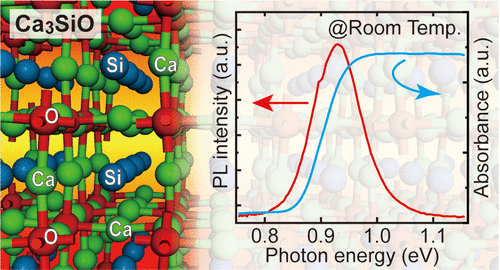
In order to discover new semiconductors free of toxic elements, the researchers took an unusual approach: they focused on crystal structures in which zinc atoms are used as tetravalent anions instead of their usual configuration as tetravalent cations. The research group chose the end of a series of experiments with oxysilicides (Ca3SiO) as well as oxygermanides in an inverted perovskite crystal structure, synthesized them, evaluated their physical properties and performed theoretical calculations. These experiments revealed that these compounds have a low energy gap of about 0.9 electron volts at a wavelength of 1.4 micrometers, findings that suggest their great potential as direct semiconductors. This feature could allow these materials to absorb, detect and emit long wavelengths in the infrared range even when embedded as thin layers, a property that would make them potential materials for use as semiconductors in the near infrared range for applications in infrared devices, such as LED devices ) and detectors.
In the future, the researchers plan to develop high-power LED devices and particularly sensitive infrared detectors through the synthesis of these compounds in the configuration of large single crystals, to develop innovative processes of growing thin layers and controlling their physical properties through doping and turning them into solid solutions. If the researchers' efforts bear fruit, then it will be possible to convert toxic components inside semiconductors into non-toxic components.
More of the topic in Hayadan:

One response
The new material operates at a wavelength of 1.4 microns - this is near infrared. The mercury-cadmium-telluride devices operate at a wavelength of 8 to 14 microns. These are completely different uses. The new material can be used for sources and detectors for optical fibers, but not for uses in the thermal field.