I met with Daniel Rosenblatt to ask him what is being done there at the university.
. The source of the image: Wikipedia, where it was uploaded by the user: Michael Schmid.")
Daniel completed a master's degree in physics at Tel Aviv University, and is currently in the middle of his doctoral thesis at the Max Planck Institute for Solid State Research in Stuttgart, Germany. He works in Prof. Klaus Kern's laboratory, and his main interest is electron tunneling microscopy. In his spare time, Daniel engages in sport climbing on walls and roller-blades.
Daniel, so what are you doing there?
The laboratory deals with a wide range of research subjects in the field of nanotechnology, physics, chemistry and materials science. The great expertise of the laboratory is in electron tunneling microscopy (scanning tunneling microscopy, STM) and its various developments.
What is electron tunneling microscopy?
When we think of microscopy we usually think of photons (light) or electrons striking the specimen, scattering and then being collected to form an imaging image. The principle of tunneling microscopy is quite different. Instead of launching particles from a distance, a very thin metallic needle is used to scan the surface of the model, a bit like a blind person reading braille (see image 1). The width of the tip of the needle is several tens of nanometers, which means it is a thousand times smaller than the diameter of a hair. During the scan, the needle is very close to the front of the model, and follows the terrain route.
The STM was first developed in the early eighties in the IBM laboratories in Zurich. The development earned the inventors, Binnig and Rohrer, the Nobel Prize in Physics in 1986.
How does the STM work?
First, close an electrical circuit between the needle and the model (see photo 1), and connect the needle to a device that will control its distance from the model with a very high level of accuracy. The needle does not touch the model and therefore electrons cannot pass between them in normal electrical conduction despite applying an electrical voltage. However, the needle is so close that electrons can pass through a process called tunneling.
What is a tunnel?
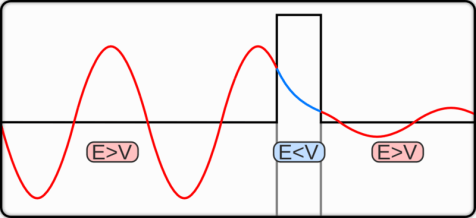
In the world of classical physics, a body that encounters an obstacle, such as a ball rolling towards a steep hill, will pass it only if it has enough energy, and in the case of the ball, speed. In the quantum world, due to wave properties, the electron has a small chance of overcoming an obstacle and appearing on the other side even if it does not have the amount of energy necessary for this (see picture 2). The thinner the obstacle, the higher the probability. The probability of a single electron tunneling from the model to the needle is very small, but the number of electrons is very large, so given the needle is close enough to the surface, enough electrons will pass so that we can measure a tunneling current. The tunnel current is very weak, so it is necessary to amplify the signal a billion times in order to be able to feed it to the computer and work with it.
Another important component of the STM system is the feedback loop whose function is to keep the needle at a constant height above the surface of the model.
How does the control circuit know the distance between the needle and the surface?
The strength of the tunneling current strongly depends on the distance between the needle and the surface, so the current is a sensitive measure of distance. The feedback loop controls the height of the needle. Its input signal is the tunnel current, and its function is to keep the current at a constant level.
So what is the output signal of the device? What are actually being measured?
The height of the needle is controlled by a piezoelectric crystal (see picture 1). These crystals produce electrical voltage in response to mechanical stress and, conversely, change their length in response to the application of electrical voltage. If the needle is connected to such a crystal (piezoelectric actuator), its height can be controlled with great precision by controlled activation of electric voltage. The voltage that is applied to the piezoelectric crystal to maintain a constant current is the output signal, that is, the signal from which the height of the surface is deduced.
What does the STM actually see?
The tunnel current depends on the electric voltage, the distance of the needle from the surface and the size called 'density of states' which is related to the density of electrons at a certain place and energy. Since we keep the voltage constant, the device maps the 'density of states' at each point. If, for example, during the measurement you move from a scan in an area of one metal to an area of another metal, the signal strength will change and in the image the area will appear at a different height because the density of states is different.
The greatest advantage of the STM is its spatial resolution which is of the order of magnitude of a single atom (see image 3). Since the tunneling current decays exponentially with distance, the bulk of the contribution comes from the transfer of electrons between the atom at the tip of the needle and the atom below it. This resolution makes it possible to study, for example, the properties of a single molecule on a metal surface.

As far as I know, commercial STM devices can be purchased. Why are you building them?
We build devices with special features or combinations of existing features that are not offered on the market. A good example of this is the project I'm working on. I am building an STM device that can also study magnetic molecules. The technique is called spin polarized STM and it is scanned with a tip that has a magnetic material at the end.
What is the purpose of the project beyond building the device?
The ambition in the memory component industry is to reduce the physical size of a bit as much as possible. A magnetic bit consists of a magnetic material that is divided into magnetically isolated complexes. A good candidate for creating a single bit of atomic size is a molecule that contains a magnetic core and an organic shell that isolates it from its neighbors. This technology is still in its infancy and has many problems for which a solution has not yet been found. But since the variety of organic molecules that can be produced is endless, we hope that he will find a combination of molecule, surface and electrical contacts that will work well together at room temperature.
The STM is an ideal instrument to study the properties of molecules on surfaces. On the one hand, it is possible to examine the effect of the surface on the shape of a single molecule and the arrangement of electrons in it. On the other hand, it is possible to check how the molecules arrange themselves on the surface when they are at a high density. As mentioned, the stability of the magnetic properties can be examined with the help of the spin polarized STM.
Our research focuses on flat molecules, which can be easily identified in a topographic image, with a metal atom in the center and various additions outside the organic ring. We are interested in finding out what types of additives preserve the magnetic properties of the central atom even at high temperatures, and how it is possible to control with their help the spontaneous arrangement of molecules scattered on a metallic surface.
In conclusion, what attracted you to this project?
One of the main things that attracted me is the challenge of designing and building the device from scratch. The project is multidisciplinary and combines work on selecting materials for low temperatures and high vacuum, designing a pump system, cooling and shock absorbing means, high frequency wiring and computerized data analysis. This is what makes the challenge great fun for me!
----------------------
I would be happy to meet and talk with any research student (maybe you?) who is willing to participate and tell me a little about what he is doing (and all for the price of a not too long conversation). You can contact me via Contact Us Form.
It's time to tell everyone what you're doing, maybe this time they'll understand too 🙂

2 תגובות
Excellent!!! Things must continue to be simplified for everyone.
Interesting interview and excellent questions, well done!