Ultra-thin lenses computer-designed from nanomaterials and "printed" in XNUMXD may eliminate the need for multiple lenses that take up a lot of space.

The camera or microscope lenses of the future will be "printed" with advanced XNUMXD printers, and will be much thinner and more precise than the lenses available today. A joint study conducted at the Weizmann Institute and Tel Aviv University, andRecently published in the scientific journal Nature Communications., describes ultra-thin lenses designed with maximum precision and manufactured from nanomaterials. These lenses will consist of several separate layers of nanomaterials, and may eliminate the existing need for multi-element lenses and replace them with a thin optical device.
For hundreds of years, the properties of lenses and the roles they play have been dictated by controlling the thickness of the material (glass) and its curvature. Later, their capabilities were further improved thanks to the combination of several lenses into one optical component. However, in the laboratory of Prof. Yachiam Pryor, in the Department of Chemical Physics at the Weizmann Institute, the optical components, including lenses, are completely different. Instead of being convex, they are based on "meta-surfaces" - materials that contain nanoscale structures that change one or more properties of light. The components are designed with the help of computer algorithms, and are manufactured with maximum precision at nanometer resolution. By changing the composition, shape, angle and position of these nanometer structures, the researchers learned to bend and shape light waves according to precise specifications.
With the help of meta-surfaces, Pryor explains, it is possible to "play" with different parameters of the light. "When lenses change the properties of light waves, they affect a feature that is rarely dealt with - the occurrence (phase), or timing, of the waves. In standard optical lenses, a defect known as chromatic aberration results from the fact that the occurrences of different light waves are inhibited unequally." When there is chromatic distortion, the lens changes the appearance differently for the different colors, and as a result the focus point of the blue, which is the short waves, is shifted from that of the red, that is, from the longer waves (a prism and a rainbow work according to a similar principle). To compensate for this deviation, even in the simplest device, lenses are composed of different elements, each of which has a slightly different focus, with the aim of correcting the deviation of one color in the image. "Up to 13 such elements may be found in a microscope or a projector. Even a cell phone will have seven, because without them, the pictures will be blurry," says Prof. Pryor.
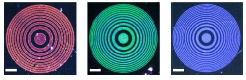
Prof. Pryor and post-doctoral researcher Dr. Euclides Almeida noticed that the meta-surfaces they were working with could be used to create a single lens with chromatic correction. The starting point of their research was based on the fact that the receptors in our eyes are prepared to receive three wavelengths, therefore, the entire digital color world is based on the synthesis of three colors - red, green and blue (the trinity known as RGB). This trinity is the basis of the electronic visual world: pixels connect the RGB components together in different ratios to recreate the illusion of the full color spectrum. In light of this, the scientists decided to develop three-layer lenses, each of which contains a metal adapted to focus a certain wavelength of light - gold for red, silver for green and aluminum for blue. Together with Prof. Tal Allenbogen and Uri Abayo, from Tel Aviv University, they found the best way to organize and produce arrays of thousands of nanometer metallic disks in thin layers, and each layer was designed separately.
The multi-layered lenses were produced using electron beam lithography technology in the clean room of the Department of Chemical Research Infrastructures at the Weizmann Institute of Science, with the assistance of Dr. Ora Bitton. In the end, the group managed to reach a relative precision in the three layers - less than 10 nanometers - an extraordinary achievement that may lead to applications where very high resolution is required. "It was no small thing to learn how to print the lenses in layers," says Pryor. "After we managed to optimize the materials we were working with for each color, and understand how the layers should be planned, the easy part came: making sure that the focal points of each layer are arranged properly."

Working in STED microscopy involves using an optical table the size of an entire lab, but in the future, it may be possible to replace the entire experimental setup with a single lens one micron thick. Of course, our research is only an initial step in this direction
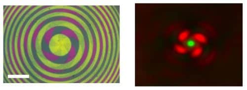
A particularly exciting future application of this technology may be in an extremely high-resolution microscope, using a microscopy method called stimulated emission depletion (STED). The method, which earned its inventor a Nobel Prize in 2014, was created to overcome the resolution limitation of conventional light microscopy - light cannot be focused to a point smaller than the wavelength of the light, which is about one micron. "The STED method," explains Pryor, "uses a nice optical trick. Usually, the entire sample needs to be excited with a laser of one color, and then it emits a certain amount of light. In the next step, this emission is mitigated, for example by projecting a ring-shaped light coming from a laser of a different color, and then a circular shape is created around the part you want to focus on. At this stage, the blocking ring is 'tightened', until the desired resolution is achieved."
The researchers hypothesize that layered lenses may make the process more accessible: "We found that it is possible to produce a distribution of light so that two colors do two different things. To demonstrate the idea, we used the image of a green dot inside a red doughnut," says Pryor. "Currently," adds Almeida, "working in STED microscopy involves the use of an optical table the size of an entire laboratory, but in the future, it may be possible to replace the entire experimental setup with a single lens one micron thick. Of course, our research is only an initial step in this direction."
Pryor explains that despite its complexity, the technique works in principle - similar to XNUMXD printing, where objects are produced layer upon layer. "Already now," he said, "we design lenses or other optical elements with the help of algorithms that are sophisticated versions of XNUMXD printing. Sitting at the computer, planning, then going down to the clean room to produce them. The accuracy, and the things we manage to do with these lenses, can only improve."
