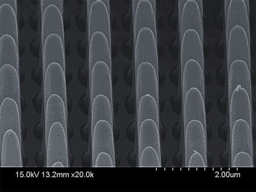
The research team developed a method for the chemical creation of arrays designed in the semiconductor gallium arsenide, the material used in solar cells, lasers, light-emitting diodes, transistors, capacitors and sensors

Manufacturing semiconductor materials for optoelectronic devices has become simpler thanks to researchers at the University of Illinois.
The research team developed a method for the chemical creation of arrays designed in the semiconductor gallium arsenide, the material used in solar cells, lasers, light-emitting diodes, transistors, capacitors and sensors. The researchers, led by Professor of Electronics and Computer Engineering Xiuling Li, published their findings in the scientific journal Nano Letters.
The physical properties of a semiconductor can vary depending on its structure, so layers of semiconductors are shaped into structures that tune their electronic and optical properties before being inserted into chips. Semiconductors can be designed using two methods: "wet" etching in which a chemical solution is used to eat the semiconductor in all directions, while "dry" etching uses a direct beam of ions that strike the surface while carving an oriented pattern. Such templates are required for quality nanostructures, or tiny shapes, with a large ratio of height to width. These structures are necessary for the development of many optoelectronic devices.
While silicon is the most common material in devices that include semiconductors, elements belonging to group III-V of the periodic table are more effective for optoelectronic applications, such as solar cells or lasers. Unfortunately, it is difficult to use these materials in a dry-eating method, since the high-energy ion beam leaves the semi-conducting surface. Group III-V semiconductors are particularly immune to this type of damage.
In order to deal with this problem, the research group utilized a method of metal-assisted chemical etching (MacEtch), a wet etching approach that the same researchers had previously developed for silicon. Unlike other wet methods, this method works in one direction, from top to bottom. This method is faster and less expensive than many of the other dry eating methods. The research group modified this method by adapting the chemical solution and the reaction conditions to the group III-V semiconductor - gallium arsenide (GaAs).
The process includes two stages - first, a thin layer of metal is placed over the gallium arsenide surface. Then, the semiconductor that includes the metal pattern is dipped in a MacEtch chemical solution. The metal accelerates the reaction so that only the areas that come into contact with the metal undergo chemical corrosion, and thus structures with a large aspect ratio are obtained. At the end of the etching reaction, the metal can be removed from the surface without damaging the semiconductor. "Being able to eat gallium arsenide with this method is a considerable achievement," notes the lead researcher.

5 תגובות
It's just the author's initial statement about the primary reason of Si inefficiencies in EO applications bugged me a little.
Ayal,
you are right about the price issue, although GaAs is more efficient it's more expensive.
In PhotoVoltaic (PV), the cell doesn't radiate, it acts as a pn junction where light (with some spectrum) excite electrons and create a potential difference (ie voltage)h
I'm not sure, but I think that the fact that Si releases phonons instead of photons still holds in PV (or more likely irrelevant)h
Maybe i went off track with my first post.... 🙂
Diodes and transistors based on gallium arsenide have been used for many years in high frequency applications and present a low noise figure - an important parameter in such applications.
Amit,
right. And yet silicone is used. At least for photovoltaic cells. It just pays, because the silicon technology is sufficiently cheap compared to the expensive production of gallium arsenide.
The statement that III-V is more efficient than Si based materials for Electro-Optic (EO) purposes is not entirely accurate. For EO the material needs to release a photon, in general. On one hand, GaAs is a direct bang gap material, which means that in order for an electron to go from the valance band to the conduction band all it needs to do is to acquire energy (and release a photon). On the other hand, Si based materials have an indirect band gap which means that an electron will have to have the same energy as before BUT also a different wave number (k) which means that the momentum must be changed (ie work/ energy is required) ; this process releases phonons by default. Hence, Si based diodes don't radiate energy like their direct band gap counterparts.