This may significantly improve the efficiency of third generation solar cells in the future

The Technion researchers from the Sarah and Moshe Zisafel Center for Nanoelectronics succeeded in polarizing a nanometer crystal by changing the composition of the molecules surrounding it. This was published in the prestigious scientific journal Nature Materials.
Doctoral student Nir Jacobi-Gross, under the guidance of the head of the Zisafel Center, Professor Nir Tessler, replaced some of the molecules attached to the surface of a numeric crystal, with molecules of a different type whose chemical group or atom linking them to the surface of the crystal is different. The researchers discovered that non-uniformity in the molecular coverage causes the crystal to be partially polarized. The group of Professor Asher Schmidt from the Shulich Faculty of Chemistry at the Technion contributed to understanding the process of linking the molecule to the crystal. As the article shows, the discovery could have far-reaching implications in significantly improving the efficiency of the solar cell. This is the third generation of solar cells that are currently under intensive development around the world, because of their relatively low cost (therefore there is a possibility of their mass production). The solar cells that are in use today are mostly based on silicon, and are expensive both in terms of their cost and in terms of the energy needed to produce them. The discovery by the Technion researchers changes the nanometer crystal's ability to receive or give electrons to the material in its environment and it is, in fact, a matter of changing the properties of the crystal.
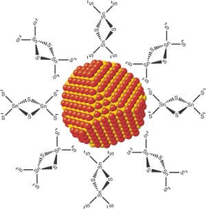
"Nano crystals from different materials are used to develop new light sources and solar cells," explains Professor Tessler. "The nano crystal is formed in a solution, its diameter is 2-8 nanometers and it is coated with an organic molecule that stabilizes it and allows the nano crystals to be dissolved in suitable liquids. In this situation, the solution is actually an ink that contains opto-electronic materials, and therefore there is currently a lot of activity in the world aimed at integrating these materials in the field of printed electronics, which will include lighting sheets or sheets of solar cells."
The researchers emphasize that in order to be able to integrate these new materials into opto-electronic devices, it is important to gain control over their properties, so that they can be treated as building blocks that are used for the engineering of an advanced device.
In the first stages of research at the Zisapel Center, it was discovered that the organic molecule could be used to shift the relative position of the particle's energy levels. What surprised the researchers at this stage, was the fact that the most important factor in this shift was the atom that is at the end of the molecule and that connects to the nano crystal. The researchers showed that it is not only possible to move the energy levels of a nanocrystal relative to other materials or nanocrystals, but that it is possible, on the same tiny nanocrystal (which is about 4 nanometers in size), to change parts of it relative to others. "This study shows that the nanocrystal, which is an inorganic island, and the organic molecules that surround it - constitute one hybrid entity of organic matter and an inorganic island," emphasizes Professor Tessler.
This distinction will require a change in the theoretical approaches that analyze these nanocrystals while ignoring the organic part (the organic molecule attached to it), usually due to the assumption that it "only contributes to the creation of a solution".
