Technion researchers have developed an innovative method to increase the efficiency of electro-optical devices such as photoelectrodes for breaking down water
Researchers at the Technion have developed an innovative method for increasing the efficiency of electro-optical devices, by increasing the interaction between light and matter. Newspaper Advanced materials It is reported that the method was successfully applied in the production of a photoelectrochemical solar cell used to produce hydrogen from water with the help of solar energy. The research was conducted by doctoral student Assaf Kay and post-doctoral student Dr. Barbara Sherer under the guidance of the head of the research group, Prof. Avner Rothschild from the Faculty of Materials Science and Engineering. The researchers developed a new method for producing metamaterials that increase the interaction between light and matter in very thin layers. These materials are made of multilayer superstructures that combine thin layers of metals and semiconducting oxides. As mentioned, the method was successfully applied in producing hydrogen from water.
Hydrogen is considered a promising fuel because its use is non-polluting. It is produced by breaking down water using solar energy in a process called photoelectrolysis. In this process, photons from the sun are absorbed by a semiconductor material and transfer their energy to electrons in the material that absorbs the radiation. These electrons are used to break down the water into hydrogen and oxygen (H2O à H2 + ½O2). This is by breaking the chemical bond between the hydrogen (H) and oxygen (O) atoms in the water molecule (H2O). The problem is that in photoelectrolysis processes, the electrons may lose the energy they received from the photons even before they had time to break down the water. This phenomenon, called recombination, affects the conversion efficiency of solar energy into hydrogen. Therefore, the need to increase the ratio between the rate of the electrochemical reaction that decomposes the water and the rate of recombination is clear.
Photoelectrolysis is carried out by photoelectrodes that absorb the light and break down the water. Those photoelectrodes are required to absorb photons in as wide a spectrum as possible and withstand hostile environmental conditions in corrosive solutions. In addition, it is important that they are produced from cheap, common and non-toxic materials. Due to the complexity of these challenges, efficient, stable and cheap photoelectrodes have not been developed for many years. In 2012, Prof. Rothschild and Dr. Chen Dotan presented, in the journal Nature Materials, the development of photoelectrodes based on iron oxide, which is a key component of rust. These photoelectrodes, which worked on trapping light in thin layers, demonstrated significant advantages over the existing ones.

However, the method published in 2012 created new challenges, related to the durability of the mirror - the reflective layer that is under the oxide. This layer is made of aluminum or silver - materials that tend to oxidize or blacken, respectively, and thus lose their effectiveness in reflecting light. At high temperatures, essential in the production of the photoelectrode, these processes are accelerated and destroy that layer. Following this, Dr. Dotan developed a multi-layered device with different layers of protection that prevent oxidation and darkening of the mirror. However, the manufacture of the device has so far been very complicated.
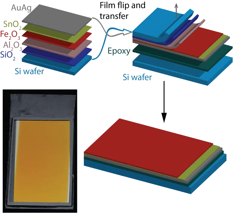
In the current study Assaf Kay and Dr. Barbara Sherer developed an innovative production method that reverses the order of deposition of the layers in the production of the device. In this method, the iron oxide is deposited on top of a piece of silicon before the metal layer above it is deposited - the mirror. This process prevents the oxidation of the metal, which can be deposited without the presence of oxygen and at a low temperature. However, the new method created a new problem: it placed the mirror above the iron oxide - contrary to the structure required in the device. Therefore, the researchers added another step in the production, in which they turn the resulting structure upside down, glue it upside down to another piece of silicon and remove the first piece of silicon to reveal the iron oxide that settles on it. (This process is described in Figure 2.)
The removal of the first piece of silicon was done by combining wet and dry etching processes used in the manufacturing process of chips for microelectronics. In these processes, utmost care is required so that the thin iron oxide, which is only about 10 nanometers thick, is not damaged. It is also important to avoid microscopic cracks that may form in this process. To this end, the Technion developed a unique production process in which protective layers of silica are used (SiO2) and alumina (Al2O3), as shown in Figure 2. This process was developed with the help of the professional staff at the Sara and Moshe Zisafel Nanoelectronics Center and the Wolfson Microelectronics Center at the Technion.
The developed process was demonstrated in the production of a photo-electrochemical solar cell for water decomposition, based on a thin layer of iron oxide (about 10 nanometers thick) on top of a stable silver and gold alloy mirror. Beyond this specific example, presented in the article published inAdvanced materials, the new process is a breakthrough in the production and development of metamaterials that combine metal layers, semiconducting oxides and insulating materials to create innovative electro-optical devices and nanophotonic structures.
The research that led to the current breakthrough was conducted under the guidance of Prof. Avner Rothschild from the Faculty of Materials Science and Engineering at the Technion, funded by the research fund (ERC) of the European Union as part of a program FP7. The researchers thank the research funds that funded the work: ERC and the Marie Curie Foundation (which financed the employment of the post-doctoral students Dr. Barbara Sherer and Dr. Daniel Garba), the Sara and Moshe Zisafel Nanoelectronics Center and the Wolfson Microelectronics Center, where the main processes in the development of the new production method took place.
More of the topic in Hayadan:

One response
The article is interesting. A few pieces of information are missing: how minute the layers are (=how commercial the method is). Are these quantum structures or micrometric layers. There is a combination of silicone with new materials - how difficult it is to grow them. If micrometrics are easy to produce and therefore the price is cheap.
What is the utility of the new cell? How much it improves the efficiency of the silicon. Silicone is common, and easy to process. The rest is not.