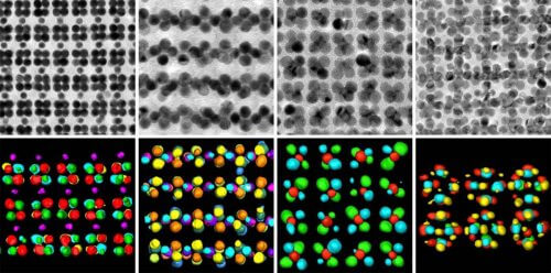
Researchers from the Weizmann Institute have developed nanoallotropes which may lead to the development of extremely small electronic devices and many other applications

Nature teaches us how important architecture is. Materials made of the same chemical element, but different in their structure, can be so different from each other that it is hard to believe that their components are identical. For example, diamonds and graphite are both made of carbon only, but differ in their atomic structure. Such structural forms of the same element are called allotropes. asRecently reported in the scientific journal Science, a research group led by Prof. Raphael Klein from the organic chemistry department of the Weizmann Institute created allotropes that do not exist in nature. These materials differ from each other not on the scale of atoms but on the nano scale: that is, in the structure of the components - which are 10 to 100 times larger than individual atoms. These allotropes of nanomaterials, called nanoallotropes, may lead to the development of ultra-small electronic devices and many other applications.
Together with the post-doctoral researcher Dr. Thomo Odiabhascararo, other group members from the Weizmann Institute and in collaboration with scientists from the United States, Spain and Belgium, Prof. Klein developed a two-step method for creating nanoallotropes. In the first step, the researchers mixed nanoparticles of gold and iron oxide into the solution, which caused the particles to self-organize into a crystalline layer above the liquid. In the second step, the scientists exposed the layer to the beam of an electron microscope, and immersed it in acid. The immersion removed the iron oxide, leaving behind only a lattice of gold particles.
The researchers discovered that when the two types of nano particles were mixed in a different ratio, different lattices were obtained. Each time the iron oxide was removed, a pure lattice of gold nanoparticles with a different internal structure was obtained - or, in other words, a different nano-allotrope of gold. The architecture of the nanoallotrope could be precisely controlled through changes in the ratio between the two types of particles.
"These materials differ from each other not on the scale of atoms but on the scale of the nano: that is, in the structure of the components - which are 10 to 100 times larger than individual atoms"
Later it became clear that, just like the classic allotropes, the nano-allotropes also differ significantly from each other. Thus, for example, they differed in their optical properties, and possibly also in electron current conductivity. Although the research was done with gold nanoparticles, it can also be applied to other materials.

The new method may help in the development of smaller electronic devices than those existing in the market. Today, the circuits that lead the electrons in the desired direction are produced by means of lithography that uses an electron beam, an extremely expensive technique that is limited in terms of resolution. The production of electronic circuits through the self-assembly of nanoparticles may reduce costs, and make it possible to build smaller devices than those produced by existing methods. Other possible applications: using nanoallotropes, it is possible to build a layer with holes of a defined size for filtration, or, alternatively, a substrate that accelerates chemical reactions, for example, in order to destroy pollutants and purify water. "Our method makes it possible to design stable, chemically resistant nanoallotropes with a predetermined structure, and it can be applied to many metals and semiconductors," says Prof. Klein.
Dr. Ronit Popovitz and Dr. Lothar Houben from the Department of Chemical Research Infrastructures of the Weizmann Institute also participated in the study, as well as researchers from the University of Antwerp in Belgium, from the Center for Collaborative Research of Biomaterials in Spain, from the University of Texas at El Paso, and from the University of Illinois at Chicago, in the United States.
#Science_Numbers
1,500,000 - the number of nanocrystals in the largest flawless array which is obtained through self-organization of nanoparticles of different sizes
