The Department of Electrical and Computer Engineering at the University of Utah succeeded in developing a vanishing device for microscopic photonic devices - the building blocks of photonic computer chips whose operation is based on light instead of electric current - this is as part of the effort to create tiny, faster and more economical chips in the future. The research findings were published in the scientific journal Nature Communications
[Translation by Dr. Nachmani Moshe]
As part of the ongoing effort to make computer chips smaller, faster and cheaper, researchers have now succeeded in creating a vanishing device for microscopic photonic devices.
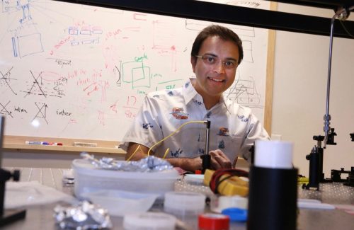
From Harry Potter's invisibility cloak to the Romulan invisibility device that made the warship invisible in the movie "Star Trek", the magical idea of an invisible object existed only in the fevered minds of MDB writers. However, Professor Rajesh Menon and his research team from the Department of Electrical and Computer Engineering at the University of Utah succeeded in developing a vanishing device for microscopic photonic devices - the building blocks of photonic computer chips whose operation is based on light instead of electric current - this is in the framework of the effort to create tiny, faster and more economical chips in the future. The research findings were published in the scientific journal Nature Communications.
The future in the fields of computers, data centers and mobile devices will involve photonic chips where data is streamed and processed as photons of light instead of electrons. The advantages inherent in photonic chips compared to the chips that are common today based on silicon are the speed of their activity and the fact that they will consume less electricity and, as a result, will heat up less. Billions of photonic devices will be embedded in each of these chips, each with a defined function, similar to the billions of transistors with different functions found in the silicon chips of our time. For example, one group of devices will perform calculations, another group will perform processing operations, etc.
The problem, on the other hand, lies in the fact that if two photonic devices are too close to each other, they will not function properly due to the fact that the light may "jump" between the two and cause interference, similar to interference in radio transmissions. At the same time, if we move them far enough apart, we will solve the problem, but the structure itself will be too big. The researchers discovered that a silicon-based nanometer barrier can be used between the two photonic devices, a kind of invisible barrier that prevents one device from affecting the other.
"The principle we use is similar to Harry Potter's invisibility cloak," said the lead researcher. "Every light beam that reaches one device is re-routed and simulates a situation as if there is no neighboring device. It is like a barrier - it pushes the light back to the original device. Thanks to this discovery, billions of such photonic devices can be packed into one chip, and thus each chip is capable of performing countless functions. And in light of the fact that these chips use photons of light instead of electrons to transfer data, their electricity consumption may be 10-100 times less, a result that will reduce the heating of the hardware, an essential advantage for information centers that use huge amounts of electricity.
The researchers believe that the most immediate application of this technology and for photonic chips in general will be in the form of data centers such as those used by major websites such as Google and Facebook. According to a study done by the US Department of Energy, in 2014 data centers in the US consumed about 70 billion kilowatt hours, or a rate of 1.8 percent of the total electricity consumption in the US. Moreover, energy consumption is expected to increase by an additional four percent by 2020. "By switching from electrons to photons, we will be able to create computers that will be much more efficient, and as a result, we will be able to reduce the carbon footprint and reduce energy consumption in all sectors," claims the chief researcher.
Today, photonic devices are mainly used in military equipment, but the researchers predict that they will reach the commercial market, and mainly data centers, within a few years.
