This basic measurement method provides important information in the way of designing and manufacturing futuristic devices and components at the atomic level: computer chips, storage systems and other devices

This basic measurement method provides important information in the way of designing and manufacturing futuristic devices and components at the atomic level: computer chips, storage systems and other devices.
About twenty years ago, a researcher at IBM's Almaden laboratories in the USA recorded a historic scientific breakthrough. The researcher, Don Eagler, proved the possibility of building tiny structures based on the maneuvering of individual atoms, each in its place. In 1989, the possibility of manipulating the individual atom, with atomic precision, was revealed to the general public for the first time. Eagler used the technology he developed to write IBM from individual atoms of the material xenon - an event whose future technological-scientific implications have been compared to those of the Wright brothers' first flight.
The current crop of innovations coming out of IBM laboratories, in collaboration with researchers at the University of Regensburg, is an important step towards measuring the tiny forces needed to manipulate the individual atom. The research findings are published in the new issue of the scientific journal Science.
Understanding the force needed to move specific atoms on a given specific surface is a key to the design and construction of tiny structures that will enable nanotechnological applications. The problem is parallel to the one faced by scientists and engineers who wanted to study and analyze the forces and rules in building larger buildings, already decades ago. Thus, for example, building a modern bridge is not possible without prior measurement of the strength of various materials expected to be integrated into it, understanding the relevant forces that will act on each part of the bridge, and analyzing the interaction between these parts. In the world of nanotechnology, placing the desired structure in a precise and permanent place on the surface requires atoms that are bound to each other in a strong bond ("sticky"), while the atoms that are requested to be mobile should be bound to each other in weaker bonds.
The results of IBM's new research provide basic information about material tissues at the atomic level, and may pave the way for the development of new generations of storage and memory components. The scientific article, entitled "The force required to move an atom across a surface", states that moving one atom of cobalt on a platinum surface requires a force of 210 pico-newtons, while moving the same atom on a copper surface exerts only 17 pico-newtons . For the sake of comparison: the force required to move a single cent copper coin weighing 3 grams is almost 30 billion pico-newtons.
The new knowledge reached by IBM scientists will enable a deeper understanding of atomic-scale processes, which are expected to be at the heart of future nanotechnological development, and its application in the fields of computing and medicine. The progress in this field is expected to provide an answer to one of the greatest challenges in the world of computing - that of the continued shrinking and miniaturization of components, transistors and circuits, at the rate predicted by Moore's Law - even at the stage when the dimensions of the conductor lines and transistors will reach the scale of individual atoms.
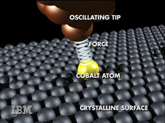
In order to measure the strength of the force needed to manipulate individual atoms, the researchers at IBM laboratories used an atomic force microscope - AFM - which measures both the strength of the force and its direction, when a tiny metal tip is used to move a single atom. The team discovered a particularly high variation, according to the type of surface on which this atom is placed.

5 תגובות
I did not understand ….
Force is a function of acceleration.
They did not say at what acceleration the atom moved after applying 210 pico-newtons.
.
.
Matan's intention, apparently, is that this is about two-dimensional movement and we are expecting the construction of three-dimensional systems, so stardust, please try to understand and not cut it off.
Have a good day
Sabdarmish Yehuda
Wait, what is a printed circuit of a chip...
And what is surface on surface...
For those who understand
In principle, all the nano circuits will be two-dimensional, meaning there will be no such structures, everything will look like a sketch on the surface???