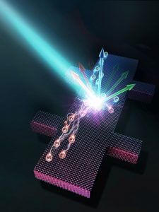
A new study published in the journal Nature, the result of a research collaboration led by IBM, describes a breakthrough. The solution enables the development of new and improved semiconductor materials

By Oki Gunawan IBM Reaserch team member
Semiconductors are the cornerstones of today's digital and electronic age. They provide us with vast amounts of devices that are useful in our modern lives, including computers, smart phones and other mobile devices. Improvements in the functionality and performance of semiconductors enable their next-generation applications for computing, sensing, and energy storage purposes. Despite this, researchers have been struggling for many years with the inability to understand how the electronic charges in semiconductor devices and the materials in advanced types of semiconductors limit our ability to achieve further progress.
A new study published in Nature magazine, the result of a collaboration led by IBM, describes an exciting breakthrough in a problem that has troubled the world of physics for 140 years. The solution allows us to give free rein to the physical properties of semiconductors in more detail and to assist in the development of new and improved semiconductor materials.
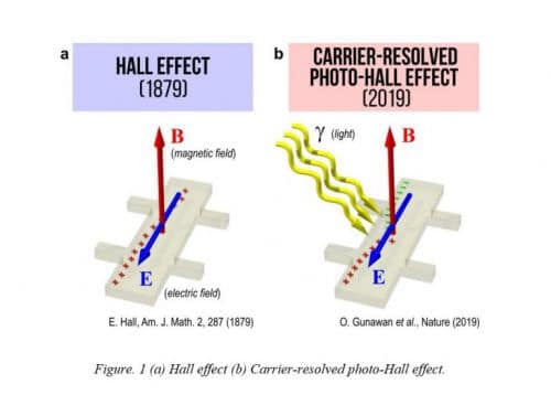
In order to truly understand the physics of semiconductors, we must first of all know the fundamental properties of the charge carriers of the various materials, know if these particles are positive or negative, what their speed is in a certain electric field and what their density is in a given material. Physicist Edwin Hall (Hall) found in 1897 a way to determine these characteristics when he discovered that a magnetic field deflects the movement of electronic charges in a conducting material and that the degree of deviation can be measured as a voltage perpendicular to the charge current, as shown in diagram 1a.. The voltage, known as the Hall Voltage , demystifies essential information about the charge carriers in a semiconductor, including whether they are negative or positive electrons or quasi-particles called "holes"? What is their speed of movement in an electric field or their "mobility" (µ) and what is their density (n) in a semiconductor?

A 140-year-old secret
Decades after Hall's discovery, researchers realized that they too could measure the Hall effect with light. The experiments they conducted were called Hall light experiments and are shown in Figure 1b.. In these experiments, the illumination with light generates in semiconductors a large number of charge carriers or pairs of "holes". Unfortunately, understanding the basic Hall effect has only provided insights into the positive charge carriers (which make up the majority of carriers). The researchers were unable to understand what the properties of both carriers are at the same time. This information is essential for many applications involving light such as solar cells and other optoelectronic devices.
The IBM Research study published in Nature explains one of the biggest puzzles of the Hall effect. Researchers from the Korea Advanced Institute of Science and Technology (KAIST), the Korea Research Institute of Chemical Technology (KRICT), and Duke University and IBM have discovered a new formula and technique that allows us to simultaneously exhaust the information on the majority and minority carriers, such as density and mobility characteristics, and also generate additional insights On the lifetime of the carriers, the length of diffusion and the process of association (recombination).
In more detail, in the Hall experiment with light, the two carriers contribute to changes in conduction (σ) and the Hall coefficient ((H, is proportional to the ratio of the Hall voltage to the magnetic field. The main insight comes from measuring the conduction and the Hall coefficient as a function of the light intensity. The conduction curve - Hall coefficient (σ- H), hidden in the conduction pathway, reveals new information: the difference in the mobility of the two carriers. The study summarizes these relationships elegantly as follows: Δµ = d (σ²H)/dσ
When the majority carrier density is known from a traditional Hall measurement in the dark, we can solve for both the mobilities and densities of the majority and minority carriers as a function of light intensity. The team called the new technique "Carrier-Resolved Photo Hall (CRPH) measurement". When the illumination intensity is known, the lifetime of the carrier can be calculated in a similar way. These relationships and their associated solutions have been hidden for nearly 150 years since the discovery of the Hall effect.

Beyond the advances made in theoretical understanding, progress in experimental techniques is also critical in order to enable the new technique. The technique requires a clean measurement of the Hall signal, a challenging task in materials whose Hall signal is weak (e.g. due to low mobility) or in the presence of additional unwanted signals such as under strong light conditions. For this there is a way to perform the Hall measurement with an oscillating magnetic field (AC). Similar to listening to the radio, the frequency of the desired station must be selected while rejecting all other frequencies that constitute noise. The CRPH technique takes us one step further and selects not only the desired frequency but also the phase of the oscillating magnetic field in a technique called "lock in detection". The concept of AC Hall measurement has been known for a long time, but the traditional technique using an electromagnetic coil system to generate an AC magnetic field was ineffective.
A discovery that foreshadows what is to come
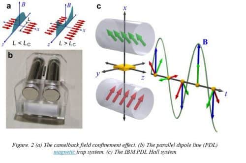
As often happens in the world of science, discoveries in one field catalyze progress in another. In 2015, IBM Research reported on a previously unknown physical phenomenon of the confinement effect of a magnetic field, this phenomenon was called the "camel's hump effect". It occurs between two crossing lines of dipoles when they exceed a critical length, as shown in Figure 2a. This effect is a key feature that enables a new type of natural magnetic trap called a parallel dipole line (PDL) as shown in Figure 2b. The PDL magnetic trap can be used as a new platform for various sensor applications such as tilt meter and seismograph (earthquake sensor).
These and other new sensing systems are being investigated by the IBM Research team developing a platform for big data analytics called the IBM Physical Analytics Integrated Repository Service (PAIRS)
Surprisingly, the same PDL component has another unique application when rotated, it serves as the ideal system for the Hall experiment in light to achieve a strong, unidirectional and harmonically pure oscillation in the magnetic field (diagram c2). More importantly, the system provides plenty of space to illuminate a large area on top of the sample, which is critical for the Hall light experiment.
the consequences
The now developed Hall light technique allows us to extract a surprising amount of information from semiconductors. Compared to only three parameters produced in the classic Hall measurement, the new technique produces up to seven parameters at each light intensity tested. These parameters include the mobility of the electron and the hole; their carrier density under light; the lifetime of the Hera-combination; and the diffusion lengths of the electrons, holes and ambipolar type. All of these can be repeated N times (that is, as many degrees of light intensity used in the experiment).
The new discovery and technology will help us promote semiconductor innovations based on existing and developing technologies. We now have the knowledge and tools to understand the physical properties of semiconductor materials in more detail. For example, we can now accelerate the development of next-generation semiconductor technology such as improved solar cells, better optoelectronic devices, and new materials and devices for artificial intelligence technology.
Sources:
[1] O. Gunawan et al., Carrier-resolved photo-Hall effect, Nature (2019).
[2] EH Hall, On a new action of the magnet on electric currents, Am. J. Math. 2, 287 (1879).
[3] "A new effect in electromagnetism discovered – 150 years later”, IBM Research Blog, , (2017); and references therein.
Oki Gunawan
IBM Research team member

6 תגובות
A nice study, whose performers completely miss its meaning...
Google-Translate would have done a better job... Is this what passes here as an article? It is quite clear that whoever wrote this does not know what he is talking about
The translation is not successful, translate the term paramobility to mobility, it should be magnetic permeability
What about a normal translation?
“Are they negative or positive electrons” – ???
“…a large number of bearers or winners of electron holes. Fortunately…”